System-Level Test for Next-Generation AI and HPC Devices
What you’ll learn:
- Complexity of AI and HPC is making system-level test more critical — and more challenging.
- Next-generation SLT must balance power, thermal, mechanical, and data demands without sacrificing cost or throughput.
- Integrated test cells provide the scalable architecture needed for tomorrow’s AI and chiplet-based devices.
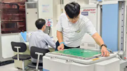
One of the primary challenges facing semiconductor manufacturers is that the devices requiring the most extensive testing are often the most expensive to test. AI accelerators, high-performance-computing (HPC) and server processors, networking ASICs, and advanced chiplet-based devices frequently require lengthy test sequences, some of which can extend from 30 minutes to more than two hours per device.
Traditional test insertions such as wafer sort and final test typically emphasize throughput. System-level test (SLT), however, must balance throughput with realistic workload execution, environmental stress, and application-level validation. This changes the economics of manufacturing test (see table).
While automated test equipment (ATE) remains essential for structural coverage and precision measurements, SLT infrastructure is designed to provide lower cost per test site through extensive parallelism. A single production SLT system may support dozens or even hundreds of concurrent test sites, allowing manufacturers to amortize infrastructure costs across large numbers of devices.
The challenge becomes particularly acute for high-volume AI processors. A manufacturer producing 1 million devices annually with a 45-minute test time may require more than 100 parallel test sites to maintain production targets. As device complexity increases, maximizing utilization and minimizing production floor space become critical design objectives for the test architecture.
Consequently, modern SLT systems are increasingly engineered as integrated production cells. Handler automation, thermal management, power delivery, software orchestration, and data collection must all work together to achieve an acceptable cost of test while maintaining coverage and reliability.
Electrical Challenges: Power Demands
The electrical demands of modern AI and HPC devices are unlike anything previously encountered in semiconductor test. High-bandwidth-memory (HBM) interfaces, advanced networking fabrics, PCI Express interconnects, and die-to-die communication links routinely operate at aggregate bandwidths measured in terabits per second. To validate these interfaces, SLT systems must recreate realistic traffic patterns while maintaining signal integrity across application boards, sockets, and test infrastructure that also provides thermal stress.
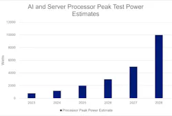
At the same time, processor power consumption continues to climb. Leading-edge AI processors are already approaching multi-kilowatt operating envelopes under peak workloads. Furthermore, industry roadmaps suggest that power requirements will continue increasing over the coming years, placing further demands on test power as well (Fig. 1).
Supporting these devices requires far more than simply supplying higher current levels. Test engineers must address power-distribution losses, voltage droop, transient response, and synchronization between device workloads and power-management subsystems. Even small variations can affect performance measurements, stability, and test repeatability.
Power delivery also becomes increasingly intertwined with thermal management. A device operating near maximum computational throughput may generate localized hotspots that shift dynamically as workloads move across processing resources. The test system must respond in real-time while maintaining stable operating conditions.
These realities are driving the development of highly integrated electrical architectures that combine programmable power systems, high-speed communications infrastructure, dynamic workload delivery, and real-time monitoring into a coordinated platform.
Mechanical Challenges: Socket Assembly
As device complexity ramps up, mechanical considerations have become a major factor in SLT system design. System-level test typically relies on socket and actuation environments that allow devices to be repeatedly inserted, exercised, and removed during high-volume production (Fig. 2). For large AI processors and chiplet-based packages, achieving and maintaining reliable electrical contact becomes increasingly difficult.
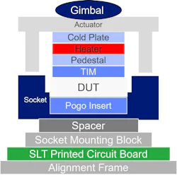
Modern packages often exhibit significant warpage due to their size, heterogeneous materials, and thermal stresses. Achieving consistent contact across thousands of signal and power connections requires highly precise mechanical alignment and substantial actuation force.
The socket assembly must be optimized to perform several functions simultaneously. It has to accurately position the device, maintain reliable electrical connectivity, support thermal transfer, and withstand repeated cycling over extended production lifetimes. In many cases, hundreds of kilograms of force may be required to ensure proper engagement between the device and the socket interface.
The challenge becomes even greater when thermal control hardware is incorporated into the socket actuation stackup. Heat spreaders, cold plates, thermal interface materials, mechanical plungers, and alignment mechanisms must operate together without compromising electrical performance or introducing mechanical instability.
Thermal Challenges: Control Loop
If electrical and mechanical challenges are significant, thermal management may be the most difficult aspect of testing next-generation AI devices. Many modern processors contain multiple compute tiles, memory stacks, networking engines, and specialized accelerators within a single package. Each element may generate heat differently depending on workload conditions, creating highly dynamic thermal profiles.
Traditional approaches based on a single temperature measurement are often insufficient. Instead, SLT systems increasingly rely on multiple temperature sensors distributed throughout the device, application board, and test environment.
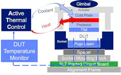
Effective thermal control requires a closed-loop architecture (Fig. 3). Internal device sensors provide junction-temperature information while external sensors monitor surrounding conditions. Software algorithms utilize active thermal control to coordinate heating and cooling systems to maintain desired operating points.
Multi-zone thermal control is becoming increasingly important. Rather than treating the package as a single thermal entity, advanced systems can independently manage multiple regions to compensate for localized hotspots and varying workload conditions.
Cooling technologies continue to evolve as well. Air-based systems remain common, but liquid cooling, refrigerant-based approaches, and hybrid thermal architectures are gaining attention as processor power levels continue to rise.
The objective isn’t simply to keep devices cool. The goal is maintaining repeatable, controlled conditions that enable meaningful performance, reliability, and power measurements throughout the test cycle.
New DFT Approaches Extend Coverage
Although SLT is often associated with functional testing, advances in design-for-test (DFT) methodology are enabling it to play an increasingly important role in structural coverage, too. Even extremely high defect coverage rates leave substantial risk when dealing with devices containing tens or hundreds of billions of transistors. Achieving incremental improvements in structural coverage through traditional methods alone can become prohibitively expensive and time-consuming.
To address this challenge, the industry is increasingly adopting techniques that allow structural test content to migrate into the SLT environment. Rather than relying exclusively on dedicated scan interfaces, newer approaches leverage high-speed communication channels such as PCI Express and USB after the device has booted. Once these interfaces are active, test software can deliver packetized test patterns, invoke built-in self-test resources, and access embedded diagnostic capabilities.
This approach offers several advantages. Existing high-speed interfaces provide abundant bandwidth, reduce dependency on dedicated test pins, and enable engineers to correlate test results across multiple phases of the product lifecycle, including design validation, production test, and post-silicon debug.
The result is a more unified test strategy that combines the strengths of traditional structural test methodologies with the realistic operating conditions available in SLT environments.
Data Infrastructure and AI-Driven Optimization
Modern system-level testing generates enormous quantities of data. Every test cycle may produce information related to performance metrics, thermal behavior, voltage margins, workload execution, communication integrity, and reliability indicators. When multiplied across hundreds of parallel sites and thousands of devices, the resulting data volume becomes substantial.
Capturing this information is only the first step. The real value lies in transforming data into actionable insights in as close to real-time as possible. To support this objective, SLT architectures increasingly incorporate networked supervisory controllers, distributed computing resources, and both centralized and distributed data-management platforms. Ethernet connectivity, cloud integration, and high-speed data pipelines make it possible for information to flow from individual test sites to factory-wide analytics systems.
Machine-learning techniques are becoming increasingly valuable in this environment. Predictive models can identify performance trends, optimize test limits, improve yield learning, and help allocate resources more efficiently. AI-based analytics may also detect subtle correlations that would be difficult to identify using conventional statistical approaches.
As the semiconductor industry moves toward increasingly autonomous manufacturing operations, real-time access to comprehensive test data will become a strategic advantage.
Integrated Test Cells: A New Architectural Model
Historically, many organizations treated system-level test as a collection of loosely connected subsystems. Power supplies, handlers, thermal controllers, software tools, and data systems were often developed and managed independently. That approach is becoming increasingly difficult to sustain.
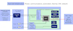
The complexity of AI and chiplet devices requires a more coordinated architecture in which all major subsystems operate as a unified test cell. Electrical infrastructure, thermal control, automation, software execution, networking, and analytics must be tightly integrated to achieve production-scale performance.
In an integrated architecture (Fig. 4), test programs coordinate with handler operations, thermal systems adapt dynamically to workload conditions, power-management resources respond to changing device demands, and data flows seamlessly between production and engineering environments.
This integration provides several benefits. It improves repeatability, reduces engineering overhead, simplifies correlation across development and production environments, and enables higher levels of automation.
Perhaps most importantly, integrated test-cell architectures provide a scalable foundation for future generations of devices whose complexity will continue to grow.
The Next Wave for SLT
Emerging innovations, such as co-packaged optics, will create new requirements for validating optical and electrical interfaces within tightly integrated systems. Device dimensions may exceed traditional handling standards. Power consumption will continue rising, placing greater demands on facility infrastructure and thermal-management technologies.
At the same time, manufacturers will face ongoing pressure to reduce the cost of test while maintaining quality, reliability, and time-to-market objectives. Meeting these demands will require continued innovation across multiple engineering disciplines. Electrical, thermal, mechanical, software, and manufacturing specialists must work together to develop test environments capable of accurately replicating real-world operating conditions at production scale.
System-level test has evolved far beyond its original role as a supplemental validation technique. For advanced AI processors, chiplet-based architectures, and future heterogeneous computing platforms, SLT is becoming a foundational element of semiconductor manufacturing. The organizations that successfully integrate power delivery, thermal management, automation, software, and data analytics into cohesive test-cell architectures will be best positioned to meet the demands of the next generation of computing devices.
>>Download the PDF of this article
About the Author
 Davette Berry
Davette Berry
VP Business Development & Customer Programs, Advantest
Davette Berry has more than 35 years of semiconductor test experience, beginning as an applications engineer and migrating to technical sales and business development. Her expertise combines electrical test knowledge with the business acumen needed for successful customer engagements. For the last 10 years, she has been instrumental in launching high-volume, semiconductor device system-level test platforms. She earned a BSEE from the University of Texas at Austin.
Comment About the Article
To join the conversation, and become an exclusive member of Electronic Design, create an account today!
 Leaders Logo
Leaders relevant to this article: