Seeing the Unseen in 3D-Stacked Semiconductors
What you'll learn:
- Key components that semiconductor manufacturers must consider in advanced packaging.
- Challenges in advanced packaging, particularly in defect analysis and die-level fault isolation.
- New technologies and techniques that ease these challenges and push the industry forward.

Today’s most advanced logic and memory chips are extraordinarily complex networks of transistors and interconnects that all must be manufactured with precision measured in fractions of a nanometer. At that scale, even atomic-level defects such as microscopic cracks buried deep in the silicon can degrade the chip’s performance — or render it unusable. While new architectures such as gate-all-around (GAA) and nanosheet transistors are sustaining the pace of device scaling, they also make structural flaws far harder to find.
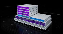
Add to that the rise of chiplets and advanced packaging approaches such as 2.5D and 3D integration, in which large silicon dies are divided into smaller chiplets and combined in a single package.
One widely deployed example is NVIDIA’s B100 Blackwell GPU. The package contains a pair of reticle-sized accelerator dies connected with high-bandwidth links and surrounded by 3D-stacked high-bandwidth memory (HBM) placed along the top and bottom edges of each die to keep data close. A single defect at the die or package levels can ripple through the entire device, complicating failure analysis as well as yield optimization.
Helping to uncover these hidden defects are more advanced microscopes that allow engineers to peer deep beneath the surface of chips. And analytical techniques such as 3D reconstruction further clarify what they’re seeing.
Electronic Design spoke with Sam Lin, Regional Marketing Manager at Thermo Fisher Scientific, about the challenges of gaining visibility into what’s happening at the die and package levels. He also explains why more advanced metrology tools are becoming critical during new process-node development as well as mass production.
What are the key components of the advanced packaging process?
Advanced packaging has earned its “advanced” designation because it represents a generational leap from traditional 2D planar chip layouts. By bonding chiplets closer together, 2.5D and 3D stacking architectures give a boost to computing power and energy efficiency while enabling a more compact footprint. These are the key drivers for high-performance applications, so that new approaches to packaging are closely aligned with market demands.
All that said, companies must contend with several common challenges, including known-good die (KGD), chiplet warpage, screening, bonding accuracy, electrostatic-discharge (ESD) protection, and, last but not least, thermal management.
First, since it can directly impact cost and throughput, identifying good dies early in the process can help ensure successful bonding. However, after the dies are dispersed into chiplets, warpage can impact the quality and precision of bonding. Because of that, it becomes critical to do real-time compensation, such as adjusting the orientation, pressure, and temperature of the bonding process. Making these adjustments early and often can be key to improving yield.
In addition, with each chip involved in hundreds of manufacturing and packaging steps, electrostatic charge accumulates. If left uncontrolled, it can cause device failure, so manufacturers must prioritize ESD protection to avoid catastrophic loss. On top of that, advanced stacking architectures can also generate substantial heat and demand more efficient thermal solutions.
What are the common challenges involved with die-level fault isolation and defect analysis? If so, how do they differ from the challenges with monolithic chip designs?
Die-level defects and faults typically originate from the semiconductor manufacturing process. For example, everything from poly/metal short circuits, silicon cracks, bridging, and particle contamination to barrier layer defects and metal shorts can directly impact device reliability and yield performance. Figure 1 shows images of several different die-level faults and defects.

In comparing multi-die and monolithic chip designs, the technical complexity significantly varies. Monolithic chip designs can consolidate components into a single silicon die. This reduces the interconnect complexity while shifting the challenges to effective thermal management and detection and isolation of defects within highly integrated structures.
On the other hand, multi-die designs elevate the risk (Fig. 2). The density and complexity of the interconnects along with advanced packaging techniques and heterogeneous integration can cause issues like electromigration, intermetallic-compound (IMC) phase orientation, void formation, thermal-management challenges, and material mismatch.
Inevitably, die-fault isolation and defect analysis are becoming increasingly complex with the rising popularity of multi-die integration. With chips that are denser and more interconnected, the smallest defects can impact the entire system in terms of performance and reliability.
Engineers and semiconductor manufacturers are turning to next-generation metrology tools and cross-disciplinary analysis methods to meet demand. By using tools that combine electrical, thermal, and structural diagnostics into one unified workflow, they can identify failure points earlier in the development cycle and support faster yield improvement and product qualification.
How can chip manufacturers overcome these challenges?
A suite of advanced metrology and analytical techniques can help address the challenges associated with die-level fault and defect analysis. The primary ones are lock-in thermography (LIT), scanning acoustic microscopy (SAM), micro-computed tomography (μCT), focused ion beam scanning electron microscopy (FIB-SEM), and transmission electron microscopy (TEM). All are key technologies for defect characterization and root-cause analysis in both monolithic and advanced packaging designs.
Non-destructive approaches to failure analysis — LIT, SAM, and μCT — are used to help evaluate interconnect integrity and identify the location and distribution of delamination, voids, and short-related defects while preserving the samples. These techniques enable powerful dimensional insights that support early fault localization and process optimization.
Semiconductor companies can use FIB-SEM to go beyond simple detection and deliver definitive root-cause evaluation by integrating high-resolution SEM imaging, precision FIB milling, and elemental compositional analysis. This makes site-specific preparation of cross-sections for detailed structural and chemical examination possible. As a result, engineers are able to quantify and visualize the nature of buried defects with greater precision, such as interfacial delamination, micro-voids, and metallization discontinuities.
FIB-SEM can also act as a gateway to atomic-scale analysis due to its ability to extract what are called “lamellae” or thin, cross-section samples of chips that engineers could then evaluate with TEM. The lamella is cut from the surface of a small sample using a focused ion beam — the FIB of FIB-SEM — and then thinned to less than 100 nm for high-resolution imaging and crystallographic diagnostics, bridging the gap between microstructural inspection and nanoscale investigation.
FIB-SEM microscopy is the cornerstone of modern failure analysis due to its ability to transform initial defect localization from non-destructive methods to a comprehensive understanding of the origins of defects and material interaction. Together, these techniques give engineers a “multi-scale” view of what’s inside next-generation semiconductor devices, ranging from macroscopic fault mapping to atomic-level defect identification.
Why is it critical to have early access to metrology and defect analysis data during semiconductor packaging development?
Early access to metrology and defect analysis data is crucial to accelerate process maturity, reduce overall development cost in packaging, and improve yield. Early access also helps transform semiconductor packaging from more of a trial-and-error development into a data-centric, precision-controlled process.
With the advancements of these packaging technologies from 2D to heterogeneous 2.5D and 3D integration, the number of process variables and failure modes increases exponentially.
Being able to receive insights into the material behavior earlier in the development process, interconnect reliability and bonding interface quality allows engineers to make reliable and data-driven decisions faster. It also minimizes risk and enables faster time-to-market, improved long-term reliability, and higher yield, which are key differentiators in the era of heterogeneous integration and advanced packaging.
What workflows best address the metrology and defect analysis challenges with the development of an advanced packaging process?
With the advanced analysis tools that are available today, the most effective way to address challenges in semiconductor packaging is to combine LIT, FIB-SEM, TEM, and μCT. These are complementary in nature, providing a complete view of how structural and electrical defects form and evolve in complex 2.5D and 3D devices.
LIT and μCT work together to uncover hidden defects buried deep within advanced packaging structures, with each method capturing a different layer of information. LIT captures active electrical or thermal anomalies with precision while the μCT uncovers the detailed 3D structure of cracks, voids, and interconnect integrity. When used together, they create a powerful, non-destructive failure analysis (FA) and quality-assurance (QA) workflow that helps chip teams detect issues faster without damaging the device.
FIB-SEM has a crucial role in preparing site-specific cross-sections and lamellae for high-resolution imaging, which enables direct observation of microstructural and interfacial features under TEM or SEM. This helps determine the root cause of electrical failures of process deviations with atomic-scale precision.
By combining LIT, μCT, FIB-SEM, and TEM, semiconductor manufacturers can have a comprehensive and complementary approach to defect analysis that covers both electrical and physical fault mechanisms. An integrated workflow supports faster and higher-throughput analysis while also ensuring structural integrity and electrothermal reliability, both of which are important for 2.5D and 3D integration and chiplet-based architectures.
Can you outline the challenges with ESD? How can advanced packaging solve some of the issues itself, and how is metrology used to support testing for long-term reliability?
As device architecture scales toward smaller geometries, increasingly heterogeneous integration, and thinner interconnects, their susceptibility to electrostatic damage rises significantly. To mitigate these risks, advanced packaging solutions are essential, not only for implementing comprehensive ESD compliance, but also for establishing QA/QC testing throughout the production process.
ESD is a hidden and growing threat in today’s semiconductor landscape. With the rise of 2.5D and 3D designs, it’s critical to build protection into the package. ESD-protective materials, optimized interconnect layouts, and conductive pathways to maintain static charges can all be integrated into the packaging platform. Materials such as antistatic dielectrics, grounded redistribution layers (RDLs), and conductive adhesives are being created to safely remove static electricity before it reaches sensitive circuitry.
With wafer-level and fan-out processes, through-package-via (TPV/TGV) design, and precise management of dielectric charging, electrostatic levels can remain below damaging thresholds.
At the same time, semiconductor manufacturers deploy inline monitoring systems that track ESD activity in real-time during key steps of chip development such as die handling, bonding, and molding. Charge-plate monitors and sensors feed data directly into QA/QC dashboards, giving engineers the insights they need in real-time to allow them to fine-tune the parameters before small issues become costly yield problems.
After the packaging stage, reliability teams begin the validation process using accelerated ESD stress models such as human body model (HBM), machine model (MM), and charged device model (CDM) testing. Next-generation packages typically embed test structures and micro-sensors to capture discharge behavior, which helps identify weak points and improve long-term reliability.
The built-in protection and monitoring align with global reliability standards that aim to ensure every package meets the strict quality expectations, such as AEC-Q100, ISO 9001, and JEDEC JESD22. With the rise of AI-driven analytics, ESD data can be leveraged for predictive reliability by training algorithms to spot the early warning signs of interconnect degradation and dielectric breakdown.
So, what used to be a reactive safeguard is becoming a more intelligent, predictive ecosystem that combines efforts in materials sciences, metrology, and machine learning to ensure chip reliability and safety.
Looking ahead, what do you think the future holds for advanced packaging technologies?
I believe that innovation will shift from transistor-level miniaturization to system-level integration, with four major trends reshaping the field: true 3D heterogeneous integration; intelligent in-line metrology; thermally adaptive materials; and sustainable, AI-driven manufacturing.
Chiplets are also moving from concept to mass adoption, with foundries, OSATs, and system integrators prioritizing open interface standards, such as UCIe (Universal Chiplet Interconnect Express) and BoW (Bunch of Wires), which enable plug-and-play interoperability among logic, memory, and analog dies across multiple vendors. What started as a solution primarily for high-performance computing and AI acceleration is quickly moving into edge processors and automotive SoCs.
At the same time, new innovations like wafer-to-wafer hybrid bonding, ultra-fine RDLs, and vertical interconnects are ushering in true 3D system-in-package (SiP) architectures. The promise of massive bandwidth and energy efficiency that comes with these technologies also introduces new reliability challenges, such as mechanical stress, thermal management, and nanoscale voiding.
Finding a solution to these challenges will require atomic-level process control, multiphysics simulation, and high-resolution metrology — tools that are defining the next generation of 3D stacking.
How is metrology evolving to handle the complexities of 3D chip architectures?
The metrology landscape is changing from a static checkpoint to a dynamic and data-driven control system. Rather than engage in post-process inspection, future lines will rely on in-situ and in-line analytics that merge FIB, SEM, X-ray, acoustic, and optical imaging data in real-time. AI-powered defect classification and machine-learning predictions will also be used before there’s an impact on yield.
With these capabilities, digital twins will become a reality, too, offering virtual representations of entire packaging flows that combine structural, thermal, and electrical data. By bridging the gap between metrology and manufacturing, fabs can self-optimize and cut cycle time while boosting first-pass yield and maintaining tighter process tolerances.
With increased device density, heat is becoming the new bottleneck. This is backed by research on low-CTE substrates, where high-thermal-conductivity dielectrics and even liquid or embedded cooling layers are emerging. Materials such as advanced ceramics and glass are gaining momentum as replacements for the organic laminates used today in high-end applications while offering superior signal integrity and thermal reliability.
The interconnect roadmap is moving beyond copper, with cobalt (Co), ruthenium (Ru), and barrierless metallization techniques being developed to overcome electromigration and resistance scaling. Simultaneously, it supports finer pitches and higher current densities that are essential for 3D logic stacks.
In what ways will sustainability fit into the future of advanced packaging?
In the sense that fabs are adopting more efficient chemistries, energy-recycling metrology tools, and closed-loop water systems in a bid to lower carbon footprints. Simultaneously, AI-driven process control is redefining production by leveraging data from failure analysis, metrology, and reliability testing. The autonomous learning systems can predict, detect, and correct issues in real-time, which helps push manufacturing closer to full self-optimization.
In the design stage, sustainability and reliability are co-optimized. The merging of EDA-DFM (design for manufacturability) with FA-Driven Design (design for analysis) enables cross-domain simulation across interposer, die, and package levels. The holistic approach enables the future of chips to be smaller, faster, smarter, more robust, and more sustainable.
In the next five years, advanced packaging will evolve from its supporting role to the central innovation engine within the semiconductor industry. The combination of 3D integration, advanced materials, intelligent metrology, and sustainability will define semiconductor teams with competitive advantages, where performance is measured by efficiency, reliability, and impact.
About the Author

James Morra
Senior Editor
James Morra is the senior editor for Electronic Design, covering the semiconductor industry and new technology trends, with a focus on power electronics and power management. He also reports on the business behind electrical engineering, including the electronics supply chain. He joined Electronic Design in 2015 and is based in Chicago, Illinois.

Sam Lin
Regional Marketing Manager, Thermo Fisher Scientific
Dr. Sam Lin is the APJ Regional Marketing Manager at Thermo Fisher Scientific, leading regional strategy and market development for semiconductor failure analysis solutions. With deep expertise in FA technologies and industry trend analysis, he drives strategic initiatives that support customers across the rapidly evolving semiconductor ecosystem.
Dr. Lin received his Ph.D. in Materials Science and Engineering from National Tsing Hua University. He began his career in 2014 as a Field Application Engineer with FEI (later Thermo Fisher Scientific), specializing in Ga⁺ and plasma dual-beam microscopy. He developed numerous automated workflows and recipes that improved analytical efficiency for major logic and memory manufacturers in Taiwan, Japan, China, and Singapore.
Comment About the Article
To join the conversation, and become an exclusive member of Electronic Design, create an account today!

Leaders relevant to this article: