Rethinking the Synchronous Rectifier in QR Flyback Converters
What you'll learn:
- How synchronous rectifier MOSFETs can affect more than just secondary-side conduction losses.
- How MOSFET capacitance and switching characteristics influence resonant behavior in QR flyback converters.
- How optimizing the synchronous rectifier can reduce primary-side switching losses and improve thermal performance.
- Practical techniques for balancing efficiency improvements with voltage overshoot management.

USB-C power adapters and other AC-DC power converters operating in the 45- to 120-W range are under constant pressure to deliver higher efficiency in ever-smaller form factors without overheating. These challenges are compounded by increasingly tight regulations for standby and active efficiency, while system designers must also meet cost and manufacturability constraints.
At these power levels, quasi-resonant (QR) flyback converters remain the most dominant topology. By enabling valley switching to reduce switching losses while maintaining a relatively simple architecture, QR flyback designs can strike a strong balance of efficiency, cost, and design complexity.
Traditionally, the primary-side switch has been the biggest loss mechanism in QR flybacks. These losses are driving engineers to adopt wide-bandgap semiconductors, specifically gallium nitride (GaN), which can use its ultra-fast switching speeds to reduce losses and the heat generated by them.
However, this has exposed a new bottleneck: the secondary-side synchronous rectifier (SR). As switching frequencies rise and conduction losses decrease elsewhere in the system, the SR increasingly dictates both efficiency and thermal behavior.
This article examines how next-generation silicon MOSFETs can be used to optimize synchronous rectification in QR flyback converters, with a focus on system-level effects. Experimental results from a 65-W USB-C reference design demonstrate how improvements in SR behavior translate directly into higher efficiency and reduced thermal stress across the entire converter.
Why the Synchronous Rectifier Has Become the New Bottleneck
In many modern QR flyback converters, the synchronous rectifier is no longer simply a low-loss replacement for the output diode. As GaN power devices drive up switching frequencies and drive down primary-side losses, the SR stage increasingly influences overall converter efficiency, thermal behavior, and switching dynamics.
Historically, SR device selection has been driven primarily by static conduction performance, with designers prioritizing low on-resistance (RDS(on)) to minimize conduction losses during the secondary current interval. Though conduction loss remains important, QR flyback converters are uniquely sensitive to the dynamic behavior of the SR device because the secondary-side switching event is tightly coupled to the resonant operation of the entire converter.
The SR device must transition rapidly and predictably in response to the transformer current while minimizing both conduction and switching losses. In practice, three device characteristics largely govern this behavior: RDS(on), gate charge (QG), and output capacitance (COSS). At the device level, these parameters are closely interrelated. Reducing RDS(on) often increases device capacitance, while improving switching speed can introduce higher voltage stress, increased ringing, or greater EMI sensitivity.
In QR flyback operation, these tradeoffs become more pronounced because switching transitions are governed by a resonant network formed by the transformer magnetizing inductance and parasitic capacitances. Therefore, the SR MOSFET influences not only secondary-side conduction loss — its capacitance and switching behavior also directly affect resonant energy transfer, transformer reset dynamics, and the voltage waveform observed on the primary side.
One important contributor is the COSS of the SR device. During each switching cycle, the energy stored in this capacitance must be charged and discharged as the transformer transitions between conduction intervals. Higher COSS increases circulating resonant energy and alters the timing of the resonant transition, which can slow drain-voltage transitions on the primary switch and increase switching losses.
Because QR flyback converters rely on predictable resonant timing to achieve valley switching, changes in SR capacitance can also shift switching timing and affect controller operation.
Figure 1 illustrates the primary drain-voltage waveform in a QR flyback converter. It highlights how resonant ringing and valley-switching behavior directly influence both turn-off overlap loss and EOSS-related turn-on loss.
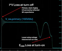
The dynamic behavior of the SR device also influences transformer reset behavior and primary-side drain ringing. Slower charge and discharge characteristics on the secondary side may increase residual energy within the resonant network, contributing to higher voltage overshoot and oscillation at the primary drain node. These effects become more important at higher switching frequencies, where even relatively small parasitic interactions can significantly affect efficiency and thermal performance.
Reverse-recovery-related effects also remain relevant, even in synchronous rectification. Although MOSFET body-diode conduction intervals are typically brief, parasitic reverse-recovery charge and nonlinear capacitance behavior can still contribute to switching losses and transient ringing during commutation.
In practical designs, the interaction between transformer leakage inductance, SR capacitance, and switching edge rates often determines whether the converter achieves clean resonant transitions or exhibits excessive overshoot and oscillation.
As a result, the SR stage can no longer be optimized in isolation or selected solely based on low RDS(on). In modern QR flyback converters, the synchronous rectifier has become an active participant in the resonant behavior of the power stage, directly influencing switching efficiency, thermal performance, voltage stress, and overall system stability.
The Evolution of Silicon MOSFET Performance
To address these system-level challenges, newer silicon MOSFET technologies have been developed that target not only lower conduction loss, but also improved dynamic switching behavior. An example is SuperQ, a next-generation silicon MOSFET architecture designed to reduce the traditional tradeoff between RDS(on), QG, and COSS that has historically constrained silicon power devices.
Unlike conventional superjunction MOSFETs, which often achieve lower on-resistance at the expense of increased capacitance and switching-related losses, SuperQ devices are designed to reduce these tradeoffs through a different charge-balanced device architecture. Traditional superjunction structures are fundamentally limited by their symmetric PN pillar geometry, in which a significant portion of the device area doesn’t contribute directly to conduction.
SuperQ instead uses an asymmetrical charge-balanced structure that enables substantially higher conduction-area utilization while maintaining high-voltage blocking capability. Figure 2 compares the two structures.
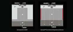
This architecture allows the device to achieve lower resistance per unit area together with higher doping concentrations and a thinner epitaxial region compared to a conventional superjunction device. The result is not only lower conduction loss, but also reduced stored charge and lower capacitive energy during switching transitions. In practical converter operation, these characteristics enable faster charge and discharge, lower switching losses, and improved resonant switching behavior.
For QR flyback applications, such dynamic improvements are particularly important because they directly affect transformer reset behavior, resonant timing, and primary-side switching conditions. Rather than simply reducing secondary conduction loss, the SR device influences how energy circulates through the resonant network during each switching cycle. Therefore, improvements on the secondary side can propagate throughout the converter, reducing primary-side switching losses. That, in turn, improves overall thermal performance.
Experimental Platform and Measurement Approach
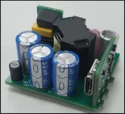
To quantify these effects, a 65-W USB-C QR flyback converter (Fig. 3) was evaluated using a UCG28826-based primary-side controller and an MPS6908 synchronous rectifier driver. The system was tested across a universal AC input range of 90 to 264 V AC, delivering a 20-V, 3.25-A output. Switching frequency varied, reaching approximately 135 kHz under maximum load conditions.
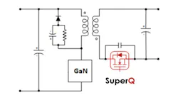
The evaluation platform allowed for a direct comparison between a next-generation silicon MOSFET (the SuperQ iS15M8R8S1C) and legacy silicon devices at the same voltage and similar RDS(on), while maintaining identical layout, control circuitry, and external components. This ensured that any observed differences could be attributed to the SR device itself. The simplified schematic is shown in Figure 4.
Efficiency Gains Reflect System-Level Interactions
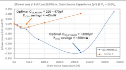
Measured efficiency exceeded 93% across the input range, with the next-generation silicon MOSFET consistently matching or outperforming conventional devices depending on operating conditions.
The efficiency and power-loss curves shown in Figure 5 illustrate that, at equivalent output power, the total power loss is reduced and efficiency is increased when using the next-generation silicon MOSFET. This reduction is particularly evident at mid-to-high load conditions, where both conduction and switching losses contribute significantly to total power dissipation.
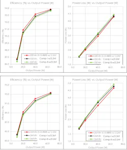
At these loads, the SuperQ device demonstrated an approximate 0.3-W reduction in total power loss, translating to a 0.2% to 0.5% efficiency improvement.
However, the most important observation isn’t the absolute efficiency number, but rather the mechanism by which it’s achieved. The reduction in total system loss can’t be explained solely by improved conduction performance on the secondary side. Instead, the data indicates a redistribution of losses throughout the converter. The differences become more pronounced at higher input voltage because switching losses increase with both bus voltage and operating frequency.
This behavior is especially significant because it demonstrates that SR optimization affects more than just secondary conduction efficiency. The observed reduction in total converter loss indicates that changes in SR switching behavior alter the resonant energy exchange of the entire power stage, lowering switching-related losses on the primary side as well.
Secondary Optimization Improves Primary Switching Behavior
One of the more significant findings from the evaluation is that the synchronous rectifier directly influences primary-side switching behavior. Although the SR is physically located on the secondary side of the converter, its capacitance and switching characteristics interact with the transformer and resonant energy-transfer process in ways that materially affect primary-side switching loss.
This interaction becomes increasingly important at higher input voltages. In QR flyback converters operating from a universal AC input, higher VIN conditions typically produce higher bulk bus voltage and a higher switching frequency. Under these conditions, switching losses increasingly dominate over conduction losses. Specifically, the turn-off overlap losses (also called I×V losses) and EOSS-related turn-on losses become a larger percentage of total converter dissipation.
The measured efficiency data reflects this behavior. At lower input voltages, where conduction losses dominate, the efficiency difference between devices is relatively modest. However, as input voltage rises, the efficiency advantage of the next-generation silicon MOSFET becomes more pronounced because the converter becomes increasingly sensitive to switching-related losses.
The mechanism behind this improvement can be understood by examining how secondary-side capacitance is reflected through the transformer during resonant operation. The SR device contributes capacitance to the resonant network formed by the transformer magnetizing inductance, leakage inductance, and parasitic node capacitances. Devices with slower charge and discharge behavior or higher stored capacitive energy increase the energy circulating within this network during switching transitions.
Using the SuperQ-based SR device, the lower stored charge and faster capacitive discharge behavior reduce the amount of residual energy present during the primary switching transition. As a result, the primary drain-source voltage transitions more rapidly during turn-off, reducing the overlap between voltage and current and thereby lowering I×V switching loss.
Such behavior is shown in Figure 6, which compares the primary switch drain-voltage turn-off transition of a superjunction SR device with that of the SuperQ SR device under identical operating conditions.
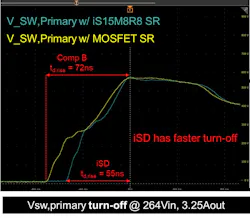
This effect was directly observed in the measurement. At VIN = 264 V AC, VOUT = 20 V, and IOUT = 3.25 A, the rise time of the primary switch node was reduced from approximately 72 ns using the conventional superjunction SR device to approximately 55 ns using the SuperQ SR device, corresponding to nearly a 25% reduction in transition time. A faster drain-voltage transition shortens the duration of simultaneous high voltage and current within the primary switch, directly lowering turn-off switching loss.
The improved resonant behavior also affected the subsequent turn-on event. Because less residual energy remained within the resonant network, the primary switch turned on at a lower drain voltage, reducing EOSS-related turn-on loss. Figure 7 shows the corresponding primary-side turn-on transition, where the lower drain voltage at turn-on decreases the energy dissipated during the charging and discharging of parasitic capacitances.
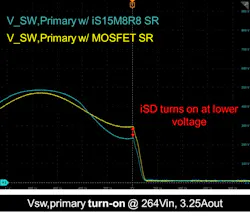
This effect becomes especially important at high VIN, where the bus voltage is elevated and the switching frequency increases, thereby magnifying the energy associated with each switching transition.
Taken together, these results demonstrate that SR optimization influences substantially more than secondary conduction efficiency alone. The SR device directly shapes the resonant switching conditions of the converter, thereby affecting primary-side switching transitions, switching-loss distribution, thermal behavior, and overall converter efficiency.
Thermal Results Highlight Redistribution of Loss
The redistribution of switching losses is also visible in the converter's thermal profile. While the SR device itself shows comparable temperature performance across devices, the most notable improvement occurs on the primary side.
At higher input voltages, the primary module temperature is significantly lower with the next-generation silicon MOSFET. In some cases, the reduction exceeds 20°C compared to legacy silicon devices (Fig. 8).
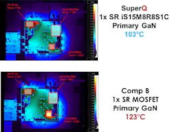
This result is particularly important because thermal limitations often constrain power density and long-term reliability. By shifting losses away from the primary switch, the overall thermal profile of the converter becomes more balanced, enabling greater performance without additional cooling.
Managing the Tradeoff Between Switching Speed and Overshoot
The improved switching speed made possible by the next-generation silicon MOSFET introduces a secondary effect of increased voltage overshoot (VPK) at the primary switch node. This behavior isn’t unique to a specific switch, but rather a natural consequence of faster transition edges within the resonant energy exchange.
The overshoot can be effectively controlled by adding drain-source capacitance across the SR device. Adjusting this capacitance slows the switching transition slightly, reducing overshoot while maintaining most of the efficiency benefit.
Importantly, this approach is equally applicable to legacy silicon MOSFETs, where adding external drain-source capacitance can also reduce switching losses and improve overall system behavior. Both devices benefit from added capacitance (Fig. 9), with an optimal value that minimizes total loss, reinforcing that this is a system-level tuning parameter rather than a device-specific requirement.
In practice, this tuning can be implemented using optional PCB pads for external drain-source capacitance. Consequently, designers are able to optimize efficiency and overshoot during converter validation.
These results suggest that synchronous rectifier selection should be treated as a system-level design decision rather than a simple conduction loss optimization. Devices that enable faster, more controlled switching behavior can reduce total system loss, even if their static parameters appear similar to those of conventional alternatives.
At the same time, designers must account for the interaction between switching speed and voltage stress. Including a provision for SR drain-source capacitance in the PCB layout provides a simple and effective means of tuning performance during validation.
A New Approach to Synchronous Rectification?
The evolution of QR flyback converters has largely been driven by improvements on the primary side, where wide-bandgap devices have enabled faster switching, greater power density, and higher efficiency. However, these gains have shifted the loss balance within the system, exposing the synchronous rectifier as a critical lever for improving system performance.
The evaluation described in this article demonstrates that next-generation silicon MOSFETs, such as SuperQ, deliver measurable improvements in efficiency and thermal performance by influencing not only secondary conduction losses, but also primary-side switching behavior.
Importantly, these improvements are achieved without altering the underlying topology or requiring new control strategies. Instead, they come from a more complete understanding of how SR device characteristics interact with the resonant behavior of QR operation.
The key takeaway is that SR optimization must be approached from a system perspective. By carefully selecting and tuning the SR device, designers can unlock improvements that extend beyond the secondary side. It enables higher efficiency, reduced thermal stress, and increased power density without requiring fundamental changes to topology or control architecture.
>>Download the PDF of this article

About the Author
Orion Kress-Sanfilippo
Systems and Applications Engineer, iDEAL Semiconductor
Orion Kress-Sanfilippo is a Systems and Applications Engineer at iDEAL Semiconductor, where he works on the development and application of advanced silicon power devices for high-efficiency power-conversion systems. In this role, he supports customers in evaluating and implementing next-generation MOSFET technologies across applications such as motor drives, battery-management systems, and high-performance power architectures.
His work focuses on bridging device-level innovation with real-world system performance, helping engineers optimize efficiency, thermal performance, and overall system cost.
Comment About the Article
To join the conversation, and become an exclusive member of Electronic Design, create an account today!

Leaders relevant to this article: