PCIe Prepares for the 3D Era
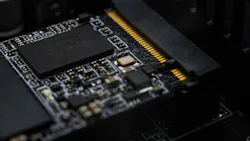
In data centers, PCI Express (PCIe) acts as a high-speed data pipeline, slinging signals between high-performance CPUs, AI accelerators such as GPUs and TPUs, and switches, memory, networking cards, and NVMe storage. Its combination of high bandwidth and low latency are both key to keeping up with the surge of data used in AI. While PCIe is still primarily used for short connections within servers, it’s increasingly being extended for longer links within racks, too.
As AI workloads strain the limits of traditional monolithic SoCs, companies aren’t simply dicing chips into heterogeneous dies called chiplets to achieve gains in speed, latency, and power. They’re also pushing data through these chips faster and adding extra PCIe lanes to move more of it, preventing the I/O from becoming a bottleneck on the system, said Manmeet Walia, executive director of product management at Synopsys.
“Compute power is growing much faster than the I/O bandwidth now,” he said in an exclusive interview with Electronic Design. “Moore’s Law is still helping logic, but the I/Os have been falling behind.”
The gap is putting pressure on PCIe and other interconnect standards to evolve faster. PCIe once progressed on a five- to seven-year cycle; now, new generations are coming out roughly every two years, with the PCIe Gen 8 spec due out in 2028.
But increasing bandwidth is not only a matter of increasing speed — as chiplets are piled into 2.5D packages and stacked in 3D, high-speed signals need to navigate dense networks of interconnects to reach the rest of the system. The higher the signaling rate, the harder it becomes to squeeze these signals through all of the noise in the package without degradation. PCIe Gen 6 doubles the signaling rate of PCIe Gen 5, making signal integrity an even tougher challenge.
Synopsys puts these challenges to the test with what it calls the first 3D PCIe Gen 6 test chip. The device delivers 64 GT/s of chip-to-chip connectivity per lane and up to 128 GB/s over an eight-lane link with PAM4 signaling (Fig. 1).
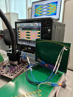
Synopsys, a leading supplier of PCIe PHYs and other IP building blocks, has worked through the challenges of PCIe Gen 6 over hundreds of implementations in traditional monolithic SoCs. The 5-nm test chip is significant, though, because it shows that high-speed PCIe IP can be implemented, packaged, and validated in 3D architectures, including designs that use face-to-face (F2F) stacking.
"PCI Gen 6 is the latest and greatest," said Madhumita Sanyal, senior director of technical product management at Synopsys. "But now we have done it in a 3D form as well with all the TSVs."
The Ties that Bind Multi-Die Chip Designs
Multi-die chip designs are trending up because they enable higher bandwidth, less latency, and better efficiency by reducing the physical distance between dies. In 2.5D packages, the dies are placed side by side and linked through interposers. In 3D, the dies are stacked vertically, reducing interconnect distance further and enabling tighter coupling between heterogeneous functions. UCIe can provide the die-to-die links inside the package.
However, the tighter integration can create challenges for getting data back out of the package. In monolithic chips, PCIe PHYs are positioned close to the perimeter of the silicon die, directly adjacent to the package’s I/O connections. Placing them on the edge of the chip shortens the high-speed traces to the package substrate, reducing signal attenuation and other forms of signal degradation. In a 2.5D package, the PHYs can similarly be positioned on the edge of the outer chiplets.
However, a 3D package adds another dimension to the problem. When chips are stacked up vertically, a PHY on the upper die can be separated from the package substrate by another layer of silicon. To address that, the I/O — including PCIe PHYs, high-speed SerDes, and high-bandwidth-memory (HBM) interfaces — is usually placed on a separate chiplet that it shares with SRAM. The most advanced logic is then arranged on a separate chiplet and stacked on top of the I/O die, with both dies usually facing the same direction.
Synopsys said the test chip uses F2F stacking technology, which is widely seen as the future for 3D chip designs. The dies are joined by hybrid bonding to create a highly dense die-to-die interface. But the arrangement requires the bottom die to be flipped so that its redistribution layer (RDL) faces the RDL of the logic above it. Thus, the PCIe PHYs no longer face the package substrate, forcing them to use vertical through-silicon vias (TSVs) to carry signals down to the package and out to the board.
"We have to start drilling holes to take the signal down to the package substrate. There is a special PDK for face-to-face, and that is what makes this complicated. We have to drill these holes and make these pathways for the signals to go down, power grounds to go down, and that leads to the complexity of the IP," said Walia.
But with the noise caused by higher interconnect densities, faster signaling rates, intricate power delivery networks (PDNs), and other complexities that come with chip stacking, new approaches are needed to implement PCIe in 3D packages.
Rebuilding PCIe for 3D Packages
Sanyal said Synopsys tackled the issues in its test chip by taking one of its previous PCIe Gen 6 chips and tearing it apart. Then, the company reassembled it with a 3D-aware architecture that preserves signal integrity from the PCIe interface to the package and out to the system board.
She added, "We tore apart the previous design and put in all the TSVs, redid the circuit design and signoff within a 3D environment using 3D PDKs, and now we have similar PCIe spec compliance successfully completed.”
The eye diagrams and other test results are important in and of themselves because receiver-jitter and other signal-integrity requirements are critical metrics for PCIe (Figs. 2 and 3). These are even more important metrics for PCIe Gen 6, which pushes more data through the same physical connection by upgrading from NRZ to PAM4. PAM4 is a more complex type of signaling, leaving less margin for losses, reflections, crosstalk, and other sources of noise and signal degradation.
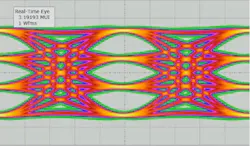
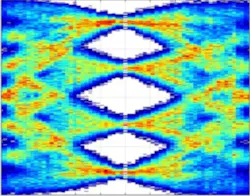
She said silicon results confirm that PCIe Gen 6 IP can operate in 3D architectures and be tested and validated against advanced-packaging and system-level requirements, especially in AI data centers.
Sanyal noted that Synopsys leaned on a lot of the same EDA tools its customers use to integrate IP into processors. Those tools support early architecture exploration, software development and system validation, multi-die and advanced-package co-design, multiphysics optimization, and die-to-die and chip-to-chip connectivity. Together, she said, they give customers a blueprint for pushing PCIe out of monolithic SoCs and into new 3D designs.
The top chiplet in the test chip is a 5-nm "dummy die" containing only what was required to validate the 3D PCIe IP. But Synopsys said some of its leading-edge customers are evaluating even more advanced "angstrom-scale" process technologies for their top dies.
According to the company, the 3D-ready IP in the test chip could be used in AI accelerators, high-performance CPUs, switches, SmartNICs, DPUs, SSD controllers, and CXL-enabled systems.
The Commercial Future for 3D-Stackable PCIe
The company will ultimately need to work closely with customers to dial in the technology for commercial silicon, said Walia. One of the challenges is accommodating the customer’s logic without interfering with the PCIe IP.
“On their top die, if they have something that is covering the bottom die in a way that it's interfering with our IP, then we have to work very tightly with the customer — to understand how much space we need to make for their logic so it can send their signals down into the package substrate," said Walia. "So, that's one area of complexity, which we have to address by working together with our customers."
He added that the other challenge is balancing the number and density of vertical connections: too few limit bandwidth, while too many can scramble each other’s signals.
The TSVs also cut directly through the die, requiring strict rules to prevent them from encroaching on sensitive areas of active silicon, and every TSV also requires a buffer or "keep-out zone" around it for the same reason.
"You rarely drill straight down into the package substrate," said Walia. "There are complex rules around it. You have to come to one of the top metal layers and then make a U-turn and then go down. We lose some flexibility as we go to 3D, and the electromigration rules and the layout rules have all changed significantly, too. All that needs to be addressed."
Further out, Walia said we will see another architectural shift with so-called 3.5D packaging. Instead of integrating PHYs and other PCIe building blocks of PCIe into the bottom die, companies could replace them with UCIe and use it to connect to a separate chiplet on the interposer. This side chiplet would act as a multi-protocol connectivity hub, providing the physical interfaces for Ethernet, PCIe, and CXL, said Walia.
About the Author
 James Morra
James Morra
Senior Editor
James Morra is the senior editor for Electronic Design, covering the semiconductor industry and new technology trends, with a focus on power electronics and power management. He also reports on the business behind electrical engineering, including the electronics supply chain. He joined Electronic Design in 2015 and is based in Chicago, Illinois.
Comment About the Article
To join the conversation, and become an exclusive member of Electronic Design, create an account today!
 Leaders Logo
Leaders relevant to this article: