The When, Where, and Why of Using Chiplets
What you'll learn:
- When, where, and why chip designers are adopting chiplets.
- Why monolithic chip designs are still the industry standard.
- The engineering challenges posed by chiplets.
- Where chiplets make the most sense today—and where they don’t.
Monolithic integration has been the dominant approach to chip design since the rise of VLSI-based ASICs decades ago. In a monolithic design, all of the building blocks of integrated circuits such as logic, memory, analog interfaces, and specialized accelerators are integrated onto a single piece of silicon. The system-on-chip (SoC) model gives engineers a compact, tightly coupled architecture with well-established design and verification flows.
However, the continued scaling of transistors and the growing complexity of systems push the limits of this approach. Modern chips are increasing in size, and the most advanced process nodes have become more expensive and yield-sensitive. As a result, fabricating all of the usual functionality of a high-performance chip on a single die can introduce significant cost, risk, and inflexibility.
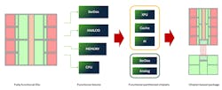
In the last 10 years or so, chiplet-based architectures have started to gain traction in the market. Rather than integrating all components onto one large die, the system is partitioned into multiple smaller dies—broadly referred to as chiplets—each optimized for a specific function. The chiplets are manufactured separately and later assembled into a single package using advanced interconnect technologies such as 2.5D packaging and 3D stacking.
While chiplets promise greater flexibility, faster time-to-market, and reduced costs, they also introduce new complexities. As a result, chiplets aren’t the best fit for every application. When does it make sense to move to a chiplet-based design? In what situations are monolithic designs the better approach? And why? This article aims to address these questions, giving engineers insights they can use to decide for themselves.
When, Where, and Why Chip Designers are Adopting Chiplets
The main drivers for choosing chiplet-based designs come down to silicon area and cost.
In the most advanced chips, particularly those used in data centers and artificial intelligence (AI), the silicon area required to fit the desired functionality on a single die can approach or exceed the reticle limit of modern lithography tools. The reticle limit is defined by the area of the photomask used in 300-mm lithography today, which measures 26 × 33 mm. That means a single monolithic chip typically can’t be manufactured larger than about 858 mm2.
>>Download the PDF of this article, and check out the TechXchange for similar articles and videos
Die size is tightly linked to what’s arguably the most critical economic reason to adopt chiplets: the cost of silicon. Fabricating large monolithic dies at advanced nodes like 5 nm or 3 nm is exponentially more expensive than at more mature nodes due to both process complexity and reduced yield. Advanced nodes require more intricate lithography, additional process steps, and higher-cost mask sets. These factors increase base manufacturing cost—even before considering yield.
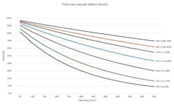
When silicon dies are large, these costs are further amplified by lower yield. The probability that a die contains one or more defects increases with the overall silicon area. So, the larger the die, the higher the risk that a significant fraction of the chips will not work. Inevitably, these non-functional silicon dies must be discarded.
Chiplet-based designs avoid this by distributing functionality across smaller dies, which have a statistically higher chance of being defect-free. Only the known-good dies are assembled into the final package. In practice, chiplet yields can exceed 50%, while large monolithic designs of similar total area may drop below 30% (Fig. 1).
Another important driver is heterogeneous integration. Many complex systems include functions with vastly different requirements, e.g., high-speed digital logic, on-chip memory, special-purpose accelerators, and low-power analog interfaces. These blocks often perform best, or most cost-effectively, on different process nodes. But in monolithic designs, all of the building blocks of IP must be implemented on the same substrate and process, often leading to compromises in performance or cost.
However, a chiplet architecture allows each subsystem to be manufactured on the best process node for the job and then integrated at the package level. Proven IP blocks from older designs, such as analog front ends, can be retained as-is, while only the critical digital logic is updated to a newer node, thus reducing development time and risk.
Chiplets also introduce modularity and reusability at the architectural level. Once a chiplet is validated and qualified, it can be reused across multiple designs without repeating the full design and verification cycle. Therefore, engineers can work faster when updating system functionality or upgrading a chip design to target different performance or feature configurations. This approach also reduces the barriers to building custom silicon for larger customers.
Finally, chiplet architectures offer advantages in scalability. New functionality can be added by integrating an additional chiplet without redesigning the entire system. If a design issue arises in a single block, only that chiplet needs to be reworked or requalified, curtailing risk and accelerating development compared to full-chip reworks in monolithic flows.
These advantages align with a growing industry vision to develop standardized chiplets that can be sourced off the shelf, enabling faster time-to-market, reduced development cost, and a competitive ecosystem of plug-and-play components.
Why Monolithic Chip Designs are Still the Industry Standard
Despite growing interest in chiplet-based architectures, monolithic ASICs remain preferred in many situations.
The main reason is architectural simplicity: integrating all functionality on a single die avoids the additional design, testing, and packaging complexities introduced by chiplet partitioning. In addition, engineers have decades of experience with designing SoCs, and they know what to look for when it comes to verification and testing. They also have access to a mature range of electronic design automation (EDA) tools, which helps cut down on the difficulties of monolithic chip development.
In addition, testing is more straightforward. Monolithic designs benefit from established design-for-test (DFT) methodologies, supported by existing tools. All functions reside on a single die, so there’s no need to coordinate tests across dies or account for potential failure modes in interconnects. This makes system-level validation more streamlined and predictable than in chiplet-based designs.
Monolithic chip designs also offer tight integration between functional blocks, minimizing interconnect latency and maximizing bandwidth. For systems with strict timing constraints—where low-latency communication between tightly coupled compute cores, or between processor cores and a shared memory block, is necessary—even small delays can degrade performance. In these cases, the physical proximity of blocks on a single die remains a key advantage.
Moreover, chiplet-based approaches introduce system-level uncertainties that are still being addressed by the industry. The challenges include establishing standards for packaging technologies and ensuring long-term reliability under thermal and mechanical stress, both of which remain active areas of development.
Testing is also in need of innovation. While chiplets are rigorously tested, they may not behave the same way after being placed in a package. Accessing individual chiplets for testing can create difficulties, too, particularly when the silicon die is positioned within a 3D stack.
Therefore, for systems that don’t push die area limits or require heterogeneous integration, the simplicity of a monolithic design may outweigh the modularity and flexibility offered by chiplets.
Choose Carefully: The Engineering Challenges Posed by Chiplets
While monolithic integration remains the more straightforward option in many contexts, the potential benefits of chiplets can warrant additional complexity. If the decision is made to move to a chiplet-based architecture, though, it comes with a new set of engineering challenges.
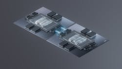
A key consideration is the partitioning strategy (Fig. 2). In other words, which functional blocks can be isolated without compromising latency, bandwidth, or timing?
The first step is to assess the technical feasibility of partitioning. Functional blocks that require tight timing or high bandwidth between them are often difficult to separate without introducing unacceptable latency. In contrast, blocks with limited interaction, such as analog versus digital logic or standalone accelerators, are generally better suited for placement on separate dies.
Another important factor is optimization of the different process nodes in the design. For instance, analog circuits typically perform to the best of their ability on more mature nodes, while digital cores benefit from advanced transistor scaling. Splitting these blocks across chiplets enables the use of advanced process technologies where they offer the most impact, without applying their associated cost across the entire design.
However, partitioning inevitably adds complexity to testing and verification. Each chiplet must be validated independently, and again as part of the assembled system, including its inter-chiplet connections. Designers may need to insert test logic at both the die and package levels, and may require separate power delivery for individual dies, making power delivery more complex than in monolithic flows. Furthermore, die-to-die interconnects introduce new failure modes and verification challenges that are still being explored across the industry.
Chip designers also need new software tools that can tackle the complexities of chiplet-based designs. While a chiplet can be designed the same way as any other monolithic chip, it’s still often challenging to examine the entire design as a single system. So, while support is improving, EDA tools for chiplet design, system-level test modeling standards, interconnect simulation, and thermal modeling aren’t yet as robust as those for monolithic design.
Universal Chiplet Interconnect Express (UCIe) and other standards aim to simplify multi-die integration. But applying these standards in practice, especially in areas such as automotive, remains formidable.
In such scenarios, strict requirements around mechanical reliability and packaging often conflict with standard interface assumptions. For example, current specifications allow for vertical via connection through the substrate, but these aren’t viable in high-reliability systems due to concerns around mechanical stress and long-term durability.
These standards not only address physical and protocol-level interoperability, but they’re also evolving to support system-level requirements such as safety, security, and testability.
On top of that, thermal and physical constraints influence how chiplets are placed within the package. Power can be distributed more effectively across a chiplet system, which may simplify cooling in some cases. But taking advantage of that depends on careful placement and routing.
Hotspots, for instance, can degrade system performance. Routing signals and power around congested areas can lead to longer interconnect paths, which may also take a toll. At the same time, physical layout constraints, such as limited substrate routing resources, could restrict how chiplets are positioned and connected.
Where Chiplets Make the Most Sense Today—and Where They Don’t
So, how do you decide between monolithic and chiplet-based integration? In the end, the decision comes down to the specifics of the application: performance requirements, system complexity, packaging constraints, cost sensitivity, and qualification requirements influence the optimal architecture.
In domains such as data centers and high-performance computing, using chiplets has increasingly become standard procedure. These systems often require large die areas to accommodate compute and memory subsystems, pushing against reticle limits and increasing the risk of yield loss.
Chiplets allow compute and memory blocks to be split across multiple dies, each potentially built on a different node, and they spread thermal load more effectively. Partitioning also enables the reuse of validated components across multiple system configurations.
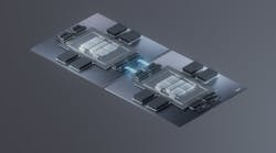
Another area where chiplet integration continues to gain traction is in automotive advanced driver-assistance systems (ADAS) and autonomous compute platforms (Fig. 3). These systems often require large, heterogeneous SoCs with strict reliability requirements.

Chiplets can help by isolating critical functions across separate dies and allowing subsystems to be tested independently before final assembly. For instance, engineers could integrate duplicate compute chiplets in a high-performance SoC to monitor each other for faults or seamlessly take over if one fails.
For now, chiplets are still relatively uncommon in the automotive industry because standards like UCIe are in the early stages of development. They have also not yet been broadly validated for mechanical robustness, thermal stress, or long-term reliability.
In contrast, other markets continue to favor monolithic integration, even at high levels of complexity. For example, in financial systems, latency is the primary concern. Even microsecond-level delays introduced by inter-chiplet communication are problematic. In this domain, large monolithic dies remain the architecture of choice, despite the higher cost, because they provide consistent performance and minimize communication delays between tightly coupled functional blocks.
Mobile and IoT devices typically favor monolithic integration, too, because they prioritize minimal size, low power consumption, and tightly integrated functionality. These requirements make the added complexity of chiplet packaging unjustified.
As packaging standards mature and system-level qualification processes evolve, chiplets may offer emerging advantages in new domains. In the aerospace industry, for instance, fault tolerance is typically achieved by using multiple redundant chips at the system level. By integrating redundancy with chiplets instead, it may be possible to reduce system complexity and improve efficiency while maintaining robustness.
Will Chiplets Become the New Standard in Chip-Making?
Ultimately, chiplets are another tool in the toolbox for chip designers. The move from monolithic chip designs to multi-die architectures is all about balancing tradeoffs shaped by design constraints, application demands, and technological maturity.
Chiplets offer compelling advantages when systems push against die-size limits, require heterogeneous integration, or benefit from modularity and reuse. In such contexts, the ability to selectively use advanced nodes and iterate more flexibly can outweigh the additional complexity posed by partitioning.
Moreover, this shift is supported by advances in packaging and substrate technology. Innovations in interposer materials, bump pitch, and routing density now make it possible to place chiplets closer together, enabling higher bandwidth, lower energy per bit, and reduced parasitics.
At the same time, monolithic integration remains the preferred option when simplicity, latency, and tightly coupled functionality are paramount. Established design flows, mature tooling, and predictable performance continue to make monolithic ASICs an efficient solution, especially for small, low-power, or latency-critical applications.
Will chiplets become the default integration strategy in the next five to 10 years? Unlikely. Chiplets represent a complementary architectural strategy, not a replacement for all design approaches. In the coming years, monolithic and chiplet-based approaches will continue to coexist, each selected based on the specific requirements of the system being built.
>>Download the PDF of this article, and check out the TechXchange for similar articles and videos
About the Author

Christopher Hunat
Package Development and Assembly Engineering Manager, imec
With over 23 years of experience in the semiconductor industry, Christopher Hunat has held key roles across several leading technology companies like Apple, Philips Semiconductors, NXP, STMicroelectronics, Socionext, and imec. He has successfully led cross-functional teams, managed complex 2.5D packaging projects, and driven innovation in areas such as substrate design, signal and power integrity analysis.
Christopher is working as Package Development and Assembly Engineering Manager, under Product Engineering (DSRD), at imec, which provides service in terms of developing a packaging solution optimized for customer design and assembly requirements.

Nidhish Gaur
ASIC Design Group Manager, imec
Nidhish Gaur works as ASIC-Design group manager at Design & System R&D (DSRD) expertise center in imec, Belgium. He has over 22 years of experience in the semiconductor industry (imec, GF, NXP, Philips, STMicroelectronics, and more). Nidhish holds a master’s degree in electronic design & technology (2003) from Indian Institute of Science (IISc), Bangalore, and a bachelor’s degree in Electronics & Telecommunication Engineering.
The ASIC-design group at imec provides ASIC design services, covering system/solution architecture (for spec-In projects), digital functional design, digital (front-end and back-end) implementation, custom layout, radiation-hardened library platform (DARE), library (re)characterization, and ASIC design project management.
Paul Zuber
Principal Member of Technical Staff, imec
In his current capacity of solution architect, Dr. Paul Zuber is an accomplished Member of the Technical Staff at IC-link by imec in Leuven, with extensive experience in project management for design and hardening of analog and digital IP blocks for space applications. He has led the development of, and contributed to, several commercial ASIC projects, including an automotive USB 3.0-C bridge and a next-generation multi-beam mask writer.
Dr. Zuber has a strong background in IC design methods, business development, and technology analysis, with numerous presentations at international conferences. He holds a Ph.D. from TU München and has published over 40 articles. His skills include various programming languages and EDA tools, and he’s proficient in multiple languages. Dr. Zuber is also actively involved in organizing conferences and social events.
Comment About the Article
To join the conversation, and become an exclusive member of Electronic Design, create an account today!

Leaders relevant to this article: