8 FPGA Standouts at electronica 2026
What you’ll learn:
- How FPGA platforms at electronica 2026 addressed robotic motion, motor protection, and deterministic sensing.
- Which FPGA development boards, sensor interfaces, and modular connections supported higher-speed embedded designs.
- How new programmable-logic applications span 4K vision, edge AI, radiation-tolerant aerospace systems, and RISC-V processing.
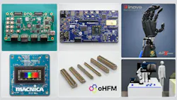
FPGA technology at electronica 2026 focused on faster processing and more precise control. Several demonstrations showed how FPGAs are being used in robotics and machine vision. One platform controlled 18 motors in a humanoid robotic hand. Another used programmable logic to process high-speed image data. Other developments included FPGA-based power protection and edge AI acceleration.
New development boards provided more options for prototyping embedded systems. High-speed interconnect standards also offered greater flexibility for modular FPGA designs. These technologies demonstrate how FPGAs can handle demanding workloads while reducing the need for conventional processors.
Table of Contents
- Inova and Lattice: FPGA Motor Control for an 18-Motor Humanoid Hand
- Samtec and Adiuvo Engineering: New Explorer FPGA Development Board
- Macnica, Sony, and Lattice: High-Speed Sensor-to-FPGA Imaging
- Vishay and Altera: Bidirectional FPGA-Controlled Electronic Fuse
- Rutronik and Altera: Agilex 5 FPGA Running Robotics and 4K Vision Workloads
- Future Electronics and Microchip: PolarFire Avalanche FPGA Development Kit
- vSamtec — Open Harmonized FPGA Module (oHFM) connectivity
- Efinix: Titanium FPGA Solutions for Edge AI and Embedded Processing
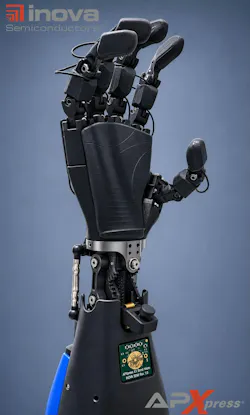
At electronica 2026 in Munich, Inova Semiconductors, Lattice Semiconductor, and the German Aerospace Center (DLR) demonstrated a distributed motor-control platform for an 18-motor humanoid robotic hand. It combines Inova’s APXpress high-speed networking with Lattice CertusPro-NX and CrossLink-NX FPGAs. This enables coordination of 18 motors, joint sensors, and a 10-sensor tactile array over a deterministic network (Fig. 1).
It completes the motion-control loop within a single 10-kHz control period. Communication latency reaches below 10 µs between sensor sampling and updated motor commands. Motors perform local field-oriented control integrated on an FPGA. A daisy-chain topology reduces wiring, preserving space around the hand’s moving joints. This technique synchronizes motor axes, reduces finger-to-finger timing skew, and enables more precise robotic manipulation.
- Lattice CertusPro-NX FPGA: Up to 100K logic cells and up to 7.3 Mb of embedded memory (EBR, LRAM)
- Lattice CrossLink-NX FPGA: Up to 39K logic cells
- 4- to 32-Gb/s selectable link rates; up to 500 virtual data channels
Samtec and Adiuvo Engineering: New Explorer FPGA Development Board
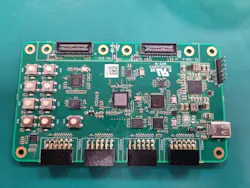
During electronica 2026 at edge lab LIVE!, Adiuvo Engineering introduced its Explorer Board. The USB-C platform, built with Samtec’s connectivity components, simplifies FPGA prototyping and high-speed interface experimentation (Fig. 2).
The board integrates four Pmod connectors using Samtec’s TSW and SSW series, along with two HSIO interfaces based on Samtec’s QSH and QSE board-to-board connectors. With this combination, developers are able to access modular peripherals and high-speed connectivity without designing a new custom board for each experiment. Engineers can use the Explorer to develop FPGA-based embedded systems applications and high-speed I/O experiments.
- On-board Raspberry Pi RP2040 MCU for power management and selected SYZYGY functions
- On-board HyperRAM for embedded and MicroBlaze V applications
- AMD Artix UltraScale+ AU7P, in an FCVA289 package
- 37K LUTs, 75K flip-flops, 216 DSP slices, and 3.6 Mb of block RAM
- Four GTH transceivers, rated up to 12.5 Gb/s
- Selected Zmod and SYZYGY modules, including the Zmod Scope, Digitizer, and AWG
- USB-C connection for power, programming, and JTAG debugging
Macnica, Sony, and Lattice: High-Speed Sensor-to-FPGA Imaging
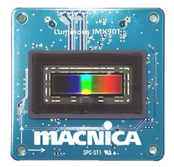
Up next is Macnica’s high-speed camera acquisition. It uses Sony’s global-shutter image sensor and Lattice Avant G/X FPGA. Image data is transferred into the FPGA for processing. This is achieved via Sony’s IMX901 sensor, Macnica’s Luminous evaluation kit, and Macnica’s SLVS-EC v3.1 Rx receiver IP (Fig. 3).
The high-bandwidth sensor stream is captured via the FPGA, which displays the processed video over HDMI. Based on the demonstration, programmable logic handles high image-sensor interface workloads and high-speed data acquisition without using a CPU.
- Sony IMX901-AMR global-shutter CMOS image sensor
- 16.41 Mpixels; 8016 × 2048 pixels
- Maximum frame rate: 134.7 fps at 10-bit output; 91.5 fps at 12-bit output
- Sensor interface: SLVS-EC, with 1-, 2-, or 4-lane configurations; up to 9.5 Gb/s per lane
- Demonstration configuration: Four-lane SLVS-EC at 9.504 Gb/s per lane
- Evaluation hardware: Macnica Luminous IMX901 SLVS-EC Sensor EVM and Luminous SLVS-EC Rx FMC Card
- Video output: HDMI, 1920 × 1080 @ 60p
Vishay and Altera: Bidirectional FPGA-Controlled Electronic Fuse
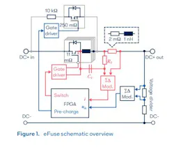
Vishay showcased a bidirectional FPGA-based electronic fuse that Altera helped develop (Fig. 4). This demonstrates that programmable FPGA logic supports protection concepts in systems with bidirectional current flow. It offers programmable control along with the potential for fast fault response in power systems.
Bidirectional protection is practical for applications involving reversible power transfer, such as battery-powered systems and advanced power architectures. Vishay also unveiled a unidirectional, MCU-based eFuse application developed with NXP.
- FPGA-based bidirectional eFuse application
- Protection concepts for bidirectional current flow
Rutronik and Altera: Agilex 5 FPGA Running Robotics and 4K Vision Workloads
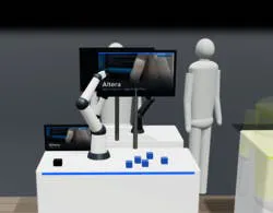
At electronica 2026, Rutronik introduced the Altera Agilex 5 FPGA SoC-based robotics and embedded-vision platform. It combines ROS2 integration, 4K camera processing, and deterministic motor control in a chip (Fig. 5).
The Agilex 5’s programmable logic deals with the sensor interfacing and preliminary camera-data processing. Then, a containerized ROS 2 software environment handles the frames. Embedded Nios V and Arm processors support higher-level operations like path planning. Robots could utilize this workload split for high-throughput vision processing and predictable real-time motion control.
- Altera Agilex 5 FPGA SoC platform
- FPGA fabric, soft processors, and Arm cores handle different workloads
- 4K camera processing, with FPGA-based sensor interfacing and preprocessing
- ROS 2 integration in a containerized software stack
- Deterministic motor control
- Nios V soft processor and Arm processor support for sensor fusion, path planning, and precision motor control
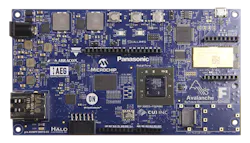
Future Electronics demonstrated the Microchip PolarFire Avalanche development kit for aerospace and other embedded systems requiring reliability. The kit uses Microchip’s PolarFire MPF300TS-FCG4841 FPGA that features 300,000 logic elements and nonvolatile configuration memory (Fig. 6).
Microchip said PolarFire FPGAs aren’t affected by single-event-effect-induced configuration upsets. This suits them for systems that get exposed to radiation, in which case, a changed configuration may cause FPGA operation interference. The board comes with connectivity and expansion options to evaluate the device in embedded systems. At the same time, Future Electronics provides bill-of-materials and engineering support for those developing systems.
- Microchip PolarFire MPF300TS-FCG484I
- 300K logic elements
- 20.6-MB embedded memory
- 924 math blocks
- SerDes supporting 250 Mb/s to 12.7 Gb/s
- 4-GB DDR3 SDRAM, 64-MB serial flash
- Gigabit Ethernet via a Microchip VSC8531 PHY; Panasonic PAN9420 Wi-Fi module
- Arduino-compatible headers, mikroBUS socket, and Pmod interface
- Embedded FlashPro5 and USB 2.0 UART
- Nonvolatile, instant-on configuration with SEU-immune FPGA configuration cells
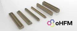
Samtec presented high-speed interconnects for the Open Harmonized FPGA Module (oHFM) standard. oHFM provides a platform-independent approach to modular FPGA systems via solderable and connector-based implementations (Fig. 7).
Defining common form factors and interfaces enables FPGA hardware development reusability and scalability. This allows developers to preserve carrier boards while upgrading processing modules or sourcing components from more than one supplier. The connector-based oHFMc modules can reach data rates of up to 112-Gb/s PAM4 per lane. The oHFM specification was announced in January 2026, which means its electronica debut showcased the standard.
- Solderable oHFM.s and connector-based oHFM.c
- Extended-length adds 20 mm to module length for additional PCB area
- Up to 64-Gb/s PAM4 per lane for Size-S and Size-M
- Up to 112-Gb/s PAM4 per lane for Size-L and Size-XL
- Supports FPGA-only and CPU-plus-FPGA designs, from entry-level FPGAs through high-performance SoC FPGAs
- High-density 0.635-mm-pitch connectors with 5- or 10-mm stack heights
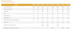
Efinix introduced its Titanium FPGA portfolio in Hall B5, Booth 150. It’s practical for applications like AI acceleration, embedded processing, and machine vision. The Titanium family features Efinix’s Quantum compute fabric, which can enhance performance, power, and area efficiency in programmable logic.
The portfolio includes FPGAs for small-scale embedded systems to complex, compute-intensive systems. Titanium devices can work with the company’s RISC-V-based Sapphire SoC solutions. Developers will then be able to combine FPGA acceleration with embedded computing.
- Efinix Titanium, including Titanium, Titanium Edge, and Titanium Transceiver series
- 35K to 2M logic elements
- TSMC 16 nm
- Proprietary Quantum compute fabric, built from configurable XLR cells
- Highly configurable 10K embedded memory blocks
- Dedicated high-speed DSP blocks: The Ti35–Ti375 devices provide 93 to 1,344 DSP blocks
- Varying transceiver options: The Ti375 supports 1.25 to 16 Gb/s per channel across four four-lane transceiver banks
- Compatible with Efinix Sapphire RISC-V SoCs, such as soft RISC-V and hardened RISC-V on devices
>>Check out more of our electronica 2026 coverage
 Electronica 2026
About the Author
 Cabe Atwell
Technology Editor, Electronic Design
Cabe is a Technology Editor for Electronic Design.
Engineer, Machinist, Cartoonist, Maker, Writer. A graduate Electrical Engineer actively plying his expertise in the industry and at his company, Gunhead. When not designing/building, he creates a steady torrent of projects and content in the media world. Many of his projects and articles are online at element14 & SolidSmack, industry-focused work at EETimes & EDN, and offbeat articles at Make Magazine. Currently, you can find him hosting webinars and contributing to Electronic Design and Machine Design.
Cabe is an electrical engineer, design consultant and author with 25 years’ experience. His most recent book is “Essential 555 IC: Design, Configure, and Create Clever Circuits”
Cabe writes the Engineering Life & Engineering on Friday blog on Electronic Design.
See Cabe's cartoons & comic strips here.

Comment About the Article
To join the conversation, and become an exclusive member of Electronic Design, create an account today!
 Leaders Logo
Leaders relevant to this article: