Evaluating Power Supplies with Different Compensation Settings
What you'll learn:
- Why switch-mode power supplies require compensation loops for stable, high-performance voltage regulation.
- Why hardware validation with actual capacitors and resistors remains critical to verify loop stability and transient performance.
- How software-controlled compensation probes replace the constant soldering and desoldering of these components, reducing evaluation time.

Power supplies are usually intended to generate a fixed, stable output voltage. The output must not oscillate, and it should remain constant with load transients and changes in the input voltage. To optimize the control loop of a switch-mode power supply, compensation pins are present in many power-supply ICs.
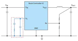
These pins can be wired with appropriate compensation components, capacitances, and resistors to optimize the control loop to achieve the highest control bandwidth while ensuring loop stability. The control loop is adjustable because the compensation needs to be approached differently depending on the operating conditions and the selection of external components in the power supply’s path. Figure 1 shows a buck regulator with a corresponding compensation pin, VC.
The external components can be selected using appropriate calculations and simulation tools such as LTpowerCAD and LTspice. However, the parasitic effects introduced by the PCB layout must also be taken into account.
As a result, every power supply design should be validated in hardware. This is one of the most time-consuming stages of the design process because it requires evaluating a Bode plot or performing load transient measurements using LTpowerAnalyzer or the like.
If the results differ from the design goals, the compensation network needs to be optimized. How that works is the existing compensation components are soldered out, and parts with different values are soldered in. And this can be a laborious process.
What’s the Point of a Compensation Probe?
One way to simplify the evaluation process is to use a compensation probe. The board in Figure 2, developed by Analog Devices, connects to the compensation and ground pins of virtually any power supply through the solder contacts on the right side of the board.
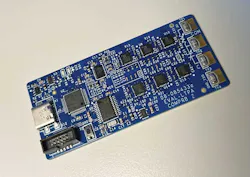
The board replaces the compensation components highlighted in the red rectangle in Figure 1. On the left side, the board connects to a PC with a USB cable. After the hardware is connected, the software for LTpowerAnalyzer can start. In it, a graphical user interface (GUI) evaluates different values for the compensation components in the shortest possible time.
Combined with an LTpowerAnalyzer, a Bode diagram can then be created, and load transient tests are able to be executed at different compensation settings.
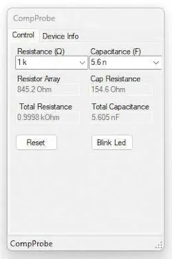
Figure 3 shows the software interface of the compensation probe. Here, engineers can select different settings, including resistance values ranging from 511 Ω to 100 kΩ and capacitor values between 5 pF and 39 nF. The internal series resistance of the capacitor could also be displayed and considered. When the compensation probe is connected to both the ground connection of the power-converter IC being tested and to the compensation pin, different compensation component values can be selected easily and quickly.
Checking and optimizing the control-loop stability of a power supply is never easy. However, a compensation probe makes it a lot easier to test different compensation settings in a reasonable amount of time. This not only helps engineers build better power supplies, but also allows them to finish designs faster.
>>Download the PDF of this article, and check out the TechXchange for similarly themed articles
 dreamstime__sergei_dolgov__173065996
About the Author
 Frederik Dostal
Frederik Dostal
Power-Management Technical Expert
Frederik Dostal is a power-management expert with more than 20 years of experience in this industry. After his studies of microelectronics at the University of Erlangen, Germany, he joined National Semiconductor in 2001, where he worked as a field applications engineer, gaining a lot of experience in implementing power-management solutions in customer projects. During his time at National, he also spent four years in Phoenix, Arizona (USA), working on switch-mode power supplies as an applications engineer.
In 2009, he joined Analog Devices, where since then he held a variety of positions working for the product line and European technical support, and currently brings in his broad design and application knowledge as a power-management expert. Frederik works in the ADI office in Munich, Germany.
Also check out my:
Comment About the Article
To join the conversation, and become an exclusive member of Electronic Design, create an account today!
 Leaders Logo
Leaders relevant to this article: