Reimagining the Image Processor for Multi-Camera Vision Systems
What you'll learn:
- The challenges placed on SoCs by multi-camera systems and the huge amounts of image data captured by them
- Decoupling ISPs from the SoC can address the fundamental issue of shared DRAM bandwidth across compute blocks
- How a DRAM-less ISP architecture can deliver sub-millisecond image processing latency.

Vision-based perception has become fundamental to everything from automotive safety systems and autonomous robots to heavy-duty drones. In each of these systems, the central challenge is the same: Raw image data from multiple cameras must be ingested, processed, and fed to AI inference pipelines with minimal latency to detect objects or other details in the surrounding area and react to them. The further challenge is staying within strict power and cost constraints.
Typically, image processing is performed within the system's main system-on-chip (SoC). But as camera counts grow and AI workloads intensify, that architecture is reaching its limits. One solution is to select a more powerful SoC, but this is expensive and it doesn’t resolve the fundamental issue of DRAM bandwidth shared across all compute blocks.
A more scalable path is to decouple image processing into one or more discrete image signal processors (ISPs), offloading the SoC so that it can focus on the tasks it was designed for: perception, sensor fusion, and decision-making. Because a discrete ISP buffers and processes image data in its own local SRAM, the image pipeline never touches the domain controller’s shared DRAM.
Pulling out the image pipeline eliminates the bandwidth contention, latency overhead, and the timing jitter caused by DRAM accesses. The result is faster, more reliable image processing for automotive, robotics, and drone vision systems.
The Challenges of Multi-Camera Vision Systems
Any system that depends on multiple camera streams for perception faces the same fundamental constraint: The central processor needs to do everything itself. It handles the raw pixel ingestion, ISP pipeline execution, and AI inference. But the challenge is executing these functions while other tasks compete for the same finite DRAM bandwidth and compute headroom. As the number of image sensors increases, this can become a design bottleneck, regardless of whether the system is a robot or a drone.
The architectural challenges of multi-camera intelligent vision systems tend to be universal. But the relative weighting of latency, scalability, and system offload varies by application:
- In safety-critical automotive ADAS, low end-to-end latency directly impacts braking distance and regulatory compliance.
- In warehouse and delivery robots, although typically operating at lower speeds, latency and jitter are critical factors that impact real-time responsiveness.
- In drones, a combination of low latency and efficient offload enables responsive flight control and rich first-person video within tight size, weight, and power (SWaP) constraints.
These systems typically use a diverse suite of sensors to safely and reliably navigate and interact with their surroundings. For design engineers developing AI-based applications, cameras and other vision sensors remain the most widely used, particularly when using sensor fusion to enable 3D spatial awareness.
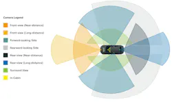
Modern ADAS functions, including emergency braking, lane departure warning, adaptive cruise control, blind spot detection, and 360-degree surround view, each carry their own set of sensor and signal processing requirements, including latency, minimum detection distance, and processor throughput. Cars equipped with ADAS systems currently use six to eight vision-based camera sensors each, as seen in Figure 1. This camera count is forecast to rise significantly with the race to more advanced self-driving vehicles.
In addition to ADAS, new in-cabin use cases, such as infotainment gesture recognition, driver and occupant monitoring, and face authentication add further camera-based processing demands to the same electronic control unit (ECU).
Autonomous mobile robots (AMRs) used in warehouses and humanoid robots deployed in factories depend on continuous, low-latency, low-jitter, visual feedback for simultaneous localization and mapping (SLAM), path planning, obstacle prediction, and manipulation. Unlike automotive, the scaling pressures in robotics are often driven not by camera count alone, but by overall system responsiveness and the pace at which new software capabilities are added on top of fixed hardware platforms.
Autonomous drones moving at high speed through urban environments require fast, precise object detection and perception. For these platforms, whether teleoperated or fully autonomous, near-instantaneous perception and video feedback are paramount for safe navigation in dense, dynamic environments. Sub-millisecond image processing reduces decision-making delays, directly improving safety during flight.
Why the SoC-Only Architecture Doesn't Scale
For any engineering team deploying multi-camera vision systems, the current architecture of performing ISP on the central SoC is unlikely to scale to meet the compute and latency demands of these systems. Maintaining synchronization across multiple video streams compounds this challenge.
When all computation blocks of the SoC share the same DRAM, increasing camera load creates resource contention that affects not just image processing, but every other workload running concurrently, including the AI inference pipeline it’s meant to serve. DRAM access is also non-deterministic by nature — access latency varies depending on competing requests, introducing timing jitter that propagates through the entire perception pipeline.
One option is to select a higher-performance SoC with sufficient resources to accommodate the required camera count. However, this is expensive, and it doesn’t fundamentally resolve the shared-resource problem. In practice, many OEMs respond by either over-specifying the SoC or adding local complexity at the edge of the system.
The alternative is to offload image processing from the domain controller SoC and perform it on a discrete ISP IC, either standalone or grouped into a sensor hub (Fig. 2). This separation has lots of upsides: the SoC's DRAM bandwidth is preserved for inference workloads; multi-camera synchronization is handled by dedicated logic rather than shared CPU cycles; and the ISP pipeline can be tuned independently of the SoC's silicon roadmap.
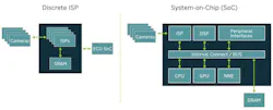
A discrete ISP is also more scalable, giving engineering teams the ability to increase camera counts while reusing a common platform. That helps keep both BOM costs and architectural complexity under tighter control.
Discrete ISP Versus Integrated SoC: How to Decide Between Them
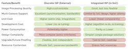
The choice between discrete and integrated ISP architectures comes down to a series of engineering tradeoffs. While priorities vary by application, discrete ISPs tend to excel in systems that need to scale camera count over time, maintain predictable latency, or support multiple product variants from a shared platform (Fig. 3).
Latency is the most consequential dimension of the discrete-vs.-integrated decision in safety-critical systems. The figures below illustrate the difference between the two architectures at a system level.
In the SoC-only architecture outlined in Figure 4, the internal ISP typically processes one camera at a time, and the AI/ML engine must wait until all frames are processed before it can begin inferencing. Delays are also caused by the DRAM read/write overhead added by ISP processing, potentially two to four extra read/write cycles. As a result, the end-to-end decision latency in a representative multi-camera system can range from 93 to 153 ms.
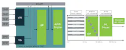
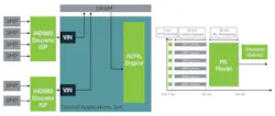
A discrete ISP processes images line-by-line from local SRAM rather than frame-by-frame from shared DRAM (Fig. 5). In this case, all cameras are available to the AI/ML engine simultaneously, with zero DRAM bandwidth consumed by the ISP stage in the domain controller. End-to-end latency is reduced to approximately 64 ms, a difference of up to 90 ms in the worst-case comparison.
The Consequences of Latency in Safety-Critical Systems
To understand the real-world significance of this difference, it helps to translate latency into physical terms across each target application:
- Automotive: A vehicle traveling at 40 mph (64 km/h) covers 1.6 feet (0.5 m) in 30 ms. At 70 mph (112 km/h), this rises to 3 feet (0.9 m). In the worst-case latency difference of approximately 90 ms between the two architectures at 70 mph, the distance covered is 9 feet (2.8 m), a gap that can determine whether an emergency braking system responds in time.
- In ADAS applications, the low, predictable latency unlocked by the discrete ISP architecture is critical for real-time safety functions such as braking, steering, and driver alerts.
- Robotics: A robot operating at 10 fps nominally sees the world every 100 ms, but an additional 50 to 100 ms of latency introduced by the ISP means vision data is outdated by an entire control cycle before any algorithm runs. For a robot moving at 1.5 m/s, this corresponds to 8 to 15 cm of unobserved motion per cycle, enough for obstacles or humans to enter the robot’s path undetected.
- In practice, latency introduced early in the image pipeline compounds across sensing and fusion stages, underscoring why, even if perception algorithms are fast, ultra-low latency ISP design is critical to preserving real-time responsiveness and safety.
- Drones: A drone operating in unstructured 3D space moves at high speeds with six degrees of freedom. Here, vision latency is often the dominant performance limiter. At speeds of 100 km/h, a 30-to 40-ms ISP delay corresponds to nearly one meter of blind flight before any autonomous control response or pilot input can occur. This compresses avoidance windows in autonomous navigation and degrades situational awareness in FPV flight.
- Reducing ISP latency yields immediate benefits in reaction distance, control stability, and autonomous safety without requiring higher frame rates, heavier compute, or algorithmic compensation.
A Scalable Solution: The Discrete ISP Sensor Hub
Moving image signal processing from the domain controller SoC to a sensor hub, equipped with one or more ISPs, increases design flexibility, enables support for a greater number of cameras, and removes high-bandwidth ISP workloads from an already resource-constrained SoC.
The ADAS sensor hub highlighted in Figure 5 supports feeds from six cameras, consolidated into two streams for the SoC. This design is built around the indie iND880 image signal processor IC, an ISP that suits a broad range of multi-camera automotive, industrial automation, and drone applications. Using a sensor hub subsystem facilitates better multi-camera synchronization and bandwidth utilization than performing these tasks on the SoC.
The SoC, freed from pixel-level processing, can dedicate its resources to the tasks that create application value: AI inference, sensor fusion, path planning, and decision-making. Critically, keeping the image processing in a dedicated ISP subsystem ensures that ISP pipeline quality and tuning remain independent of the SoC's dynamic workload, producing higher-quality, more consistent input to downstream AI algorithms that run inside the car’s domain controller.
Offloading ISP tasks applies equally to autonomous robots, where the SoC focuses on path planning and obstacle prediction while the ISP subsystem handles all image pre-processing. Latency, timing jitter, and sensor synchronization are first-order design constraints in AMRs, because even small variations in sensor timing can undermine perception quality, sensor fusion, and closed-loop control. Low-jitter vision pipelines simplify synchronization with IMUs, odometry, and other sensors, and reduce the need for compute-intensive software compensation.
This determinism is a direct consequence of a DRAM-less ISP architecture. Without competing DRAM accesses, image delivery timing becomes predictable and bounded. Within this context, resource offload becomes a key enabler: As OEMs continuously refine and add software behaviors such as navigation, object detection, obstacle avoidance, and telepresence within fixed power and compute budgets, a discrete ISP supports multi-camera integration without forcing a costly SoC upgrade or increasing end-to-end latency.
The same scalability benefit that allows automotive OEMs to reuse sensor hubs between models applies directly to a robotics OEM building multiple product tiers on a common hardware platform.
In drones, low-latency vision ensures fast response for obstacle avoidance, flight control, and first-person viewing, especially in dense, dynamic environments. Offloading ISP tasks is particularly valuable given tight SWaP constraints and limited CPU/GPU headroom. Scalable support for stereo and multi-directional cameras allows OEMs to offer richer situational awareness or higher autonomy levels with minimal changes to the flight-control compute platform.
How ISPs Can Help Stay Ahead of Sensor Proliferation
The proliferation of cameras across automotive, robotics, and drone platforms isn’t a future trend. It’s the present reality. As AI competes for more memory and clock cycles and more cameras are embedded into these systems, the central SoC can no longer be the default for image signal processing. The shared-resource bottleneck is already a design constraint, and it will only become more acute in the age of fully autonomous cars, automated production lines, and humanoid robots.
Decoupling image signal processing into a dedicated discrete ISP, or a sensor hub built around one or more ISPs, addresses the three core design constraints simultaneously:
- It reduces end-to-end decision latency by eliminating ISP processing from the SoC's job description.
- It frees up DRAM bandwidth and compute resources for the AI workloads.
- It provides a more scalable, SoC-independent platform that OEMs can reuse in different designs.
Rather than take the costly route of continually over-specifying the SoC to manage additional cameras, discrete ISPs provide a more viable, more flexible, and more future-proof architecture.
>>Download the PDF of this article, and check out the TechXchange for similarly themed content
 dreamstime_dashark_184164716
 promo_alexandr_yakevlev_dreamstime_xxl_267692611
About the Author
 Dinesh Balasubramaniam
Dinesh Balasubramaniam
Director, Product Marketing, indie Semiconductor
Dinesh Balasubramaniam is indie’s Director of Product Marketing for robotics and AI/ML solutions, responsible for business development and product marketing for the company’s camera video processors and vision-based products and solutions.
Prior to joining indie in 2024, he held various roles at Ambarella Inc., including Sr. Manager, Product Marketing and Director, Product Applications Engineering. In these roles, he led technical marketing and applications engineering for the AIoT business unit, supporting the full customer lifecycle from pre-sales engagement through post-sales support for Ambarella’s global customer base.
Before that, Dinesh was Staff Software Engineer at Dolby Laboratories, where he worked on end-to-end product development of professional communication hardware, focused on system architecture, software development, and product manufacturing. Prior to that, he served as an Applications Engineer at Maxim Integrated Products.
Dinesh holds a Master of Science in Electrical Engineering, specializing in Signal Processing from the University of Texas, Dallas, and a Bachelor of Engineering, Electronics and Communications Engineering from Bharathidasan University in India.
Comment About the Article
To join the conversation, and become an exclusive member of Electronic Design, create an account today!
 Leaders Logo
Leaders relevant to this article: