GaN FET Uses Dual-Side Cooling to Deliver 800-V Power to AI

The problem with packing over 100 kW into a single AI rack is about more than delivering power. Space and heat have become critical factors for the power electronics that convert and distribute it all.
While most power FETs still use conventional top-side-cooled packages, dual-side cooling (DSC) is emerging as an alternative. These double-sided packages dissipate heat from both the top and bottom of the device, enabling smaller form factors while reducing top-side thermal impedance.
"Customers building megawatt-scale AI data centers are running out of board space and thermal headroom before they hit their power limits," said John Wiggenhorn, senior product line director of high-voltage GaN at Renesas.
To tackle these challenges, specifically in data centers, the company introduced what it called the first 650-V GaN device with dual-side cooling. The TP65H020G4PLSGBD is targeted at the high-density DC-DC converters used in 800-V architectures.
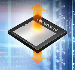
Featuring only 20 mΩ of on-resistance (RDS(on)), the new device comes in a compact 8- × 8-mm PQFN package that’s approximately 60% smaller than the 10- × 15-mm TOLT package it’s replacing. By using dual-side cooling, the GaN power FET can remove heat from both sides at the same time, reducing top-side thermal impedance by 10% and improving its performance in densely packed server racks such as AMD’s Helios.
High-Voltage GaN for High-Voltage DC Power Trends
Renesas said the device is “purpose-built” to meet the rising power demands of GPUs and other AI chips, which are exposing a lot of inefficiencies with how power is traditionally moved up and down the rack.
As rack power climbs from roughly 120 kW into the megawatt range, NVIDIA and other AI giants such as Google, Meta, and Microsoft are backing a broader shift to high-voltage DC (HVDC) architectures. By using an 800-V DC bus, the current racing around the compute rack can be significantly reduced, which in turn reduces the copper needed to distribute it all and the power losses that occur on the way. That reverses many of the space, heat, and other penalties that come with the 48-V bus.
In the short term, AC-DC power supplies in the compute rack will be relocated into dedicated power racks reclaiming rack space for more AI accelerators and other hardware. These sidecar racks convert 480 V or other high-voltage AC to 800 V DC and then shoot the power over to the compute rack using busbars, potentially liquid-cooled. In most cases, power will be distributed up and down the rack at 800 V before a DC-DC converter inside the server steps it down.
The new GaN FET is targeted at these board-level intermediate bus converter (IBC) stages that step down 800 V to 48 V, 12 V, or 6 V DC. It can also be used in the battery backup unit (BBU) stages of sidecar racks.
Dual-Side Cooling Pushes More Power Through Smaller Packages
The device draws on the capabilities of Renesas’ Gen IV Plus GaN architecture: low gate charge and output capacitance, a built-in freewheeling diode with minimal reverse recovery, and a high threshold voltage that runs without a negative gate bias. As a depletion-mode (D-mode) device, standard silicon gate drivers can be used to drive it. As a result, it can switch at frequencies above 1 MHz without requiring the more advanced gate drivers used with enhancement-mode (E-mode) devices. Faster switching speeds save PCB space by shrinking passive components.
Wiggenhorn added, “We cool the device from both sides and cut the footprint significantly, so designers can move more power through the intermediate bus without redrawing the board or adding more cooling hardware. And because it keeps the operational simplicity of the silicon gate-drive customers already use, it's an extremely easy upgrade." Renesas is currently sampling the device to OEMs and ODMs in the AI data center market.
The company said it has already validated the approach in silicon. A 6-kW LLC DC transformer reference design uses the 650-V GaN FET to efficiently convert the 800-V DC bus to 48 V DC, reaching 2.6 kW/in.³ of power density while providing galvanic isolation. The DC-DC converter utilizes a multilevel architecture that can handle the higher voltages required by 800-V architectures by stacking several lower-voltage GaN FETs in series.
Instead of exposing a single switch to the full voltage, each device in the multi-level converter handles only a fraction of the total voltage, giving engineers the flexibility to use 650-V GaN instead of devices rated for more than 1,000 V, which are still relatively scarce. The reference design also leverages Renesas’ RA6T3 MCU — it offers 200-MHz operating frequency and 256 kB of flash and 40 kB of SRAM to execute the more complex control algorithms used by multi-level converters.
According to Renesas, the IBC delivers 0.21% higher efficiency at full load than an equivalent TOLT-based board. The smaller package also reduces PCB area and enables a more tightly matched layout across the FETs.
Renesas is also leveraging the new DSC 8x8 device in 800- to 12-V and 800- to 6-V DC-DC IBC reference designs. The device will be on display at the OCP Global Summit this month in San Jose, California.
About the Author
 James Morra
James Morra
Senior Editor
James Morra is the senior editor for Electronic Design, covering the semiconductor industry and new technology trends, with a focus on power electronics and power management. He also reports on the business behind electrical engineering, including the electronics supply chain. He joined Electronic Design in 2015 and is based in Chicago, Illinois.