The Step-by-Step Process of STCO
What You'll Learn
- How system-level technology co-optimization (STCO) helps engineers optimize power, performance, area, cost, and reliability
- Howdigital twins and multiphysics analysis can help streamline multi-die development across chiplets, packages, interposers, and boards.
- How chiplet-based systems are verified and validated, from DFT and assembly verification to UCIe compliance and signal-integrity analysis.
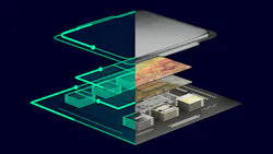
Building bigger chips is no longer the only way to build better ones.
By assembling heterogeneous chiplets onto interposers and advanced packages, engineers can achieve levels of performance, power efficiency, and scalability that are difficult to reach with traditional monolithic designs. The tradeoff is complexity. Designing chips comprised of multiple dies, often packed with both third-party and proprietary IP, creates challenges that single-die design tools are not equipped to solve.
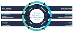
To harness the full potential of chiplets, the broader industry is moving to a more system-centric approach known as system-level technology co-optimization (STCO). Rather than optimizing every layer of the chip design independently, STCO considers the interactions between silicon, package, interposer, and PCB from the start (Fig. 1). By adopting EDA tools that can take such a system-level view, engineers can optimize power, performance, area, and cost (PPAC) as well as reliability and safety across all domains at the same time.
By integrating all the layers of the 3D IC into the same workflow, STCO helps engineers understand how decisions made in one domain affect every stage of the integration process. It also provides early, predictive insights into the eventual performance of the chip design. This shift-left approach is critical for cutting down on iterative design cycles, which can mean a major boost to engineering productivity.
Constructing the 3D Digital Twin
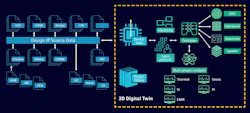
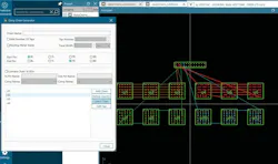
A streamlined multi-die design process starts with creating a complete 3D digital twin of the entire device assembly. This begins with the aggregation of diverse design IP to construct a full-system model, which serves as the single, authoritative source of system connectivity. This digital twin drives the creation of interfaces and bump arrays for chiplets, bridges, interposers, and substrates (Fig. 2).
Pulling together all the data presents significant challenges, as manual processing is inherently error-prone and lacks the repeatability required for hyperscale-class chip designs.
While standard formats such as IEEE 3Dblox, OCP CDX, and JEDEC JEP30 are emerging to ease collaboration, engineers still often encounter randomized data formats. As a result, effective data management and robust revision control are key, and the methodology should seamlessly integrate new IP versions without overwriting existing work while maintaining a consistent netlist. This is crucial for subsequent layout versus schematic checks, logical equivalency checking, and multiphysics analysis.
Advanced Connectivity and Hierarchical Planning
Driven largely by the demands of AI computing, modern chip designs often feature more than 50 million total pins and hundreds of thousands of connections, rendering traditional approaches to connectivity management obsolete.
To manage this explosion of die-to-die connections, designers are increasingly adopting language-based design. Writing Verilog RTL with proper bus notation is significantly more efficient and less error-prone than bit-by-bit spreadsheet definitions, which cannot scale to the millions of bumps required by hybrid and direct bonding technologies.
Hierarchical design further simplifies this complexity by disaggregating the system into manageable building blocks. By representing devices as hierarchical entities, designers can define topological pin regions using formulas, regular expressions, and design attribute tokens. Intelligent parametric pin regions enable the rapid creation and optimization of complex package designs. This allows for the efficient instantiation of silicon bridges and interposers, which act as low-latency, power-efficient wiring layers between CPUs, GPUs, and high-bandwidth memory (HBM) stacks.
Pathfinding and Predictive Multiphysics Analysis
A critical aspect of STCO is the ability to perform pathfinding, which means exploring different integration scenarios that align with the PPAC targets for the design.
To do this, engineers need to be able to view and manipulate all the building blocks of the system, including mechanical objects like heat spreaders and stiffeners, within a single cockpit. This allows for early assessment of how mechanical parts impact real estate and electrical clearances.
Predictive analysis is what makes or breaks this pathfinding process. For example, planning a power delivery network requires "shift-left" analysis to identify DC-drop issues early, prioritizing problem detection over absolute sign-off accuracy to prevent costly late-stage changes.
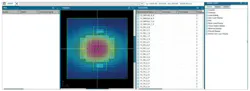
Similarly, early thermal evaluation is imperative in 3D ICs. Vertical chiplet stacking restricts traditional heat-removal paths through the top and bottom of the die. At the same time, thinning the dies increases lateral thermal resistance, making it more difficult for heat to escape through the sides of the chip. By using 3D-optimized EDA tools, engineers can model thermal gradients and mechanical stress across the entire assembly, ensuring that co-design optimizations do not introduce unmanageable reliability challenges.
Comprehensive Testing and DFT Strategies
Once co-design optimization is complete, the focus shifts to comprehensive testing. While die-level testing remains consistent with 2D processes, 2.5D, and 3D IC packages require special die-to-die interconnect testing and stack-level verification. A robust 3D IC design for test (DFT) solution extends hierarchical DFT principles to the stack level.
To maintain efficiency, pattern generation is typically performed at a lower level of hierarchy and then retargeted to the die-top and stack-level “top” for testing. This ensures that time-consuming automatic test pattern generation is only executed once. Furthermore, an effective DFT solution must account for unintended thermal effects during testing, as the heat generated by testing one die can impact the performance of adjacent dies in the stack.
Formal Sign-off and Assembly Verification
The final stage of the workflow is formal sign-off, a process made more complex by the integration of chiplets from multiple process nodes and foundries. The absence of a unified, formal verification process has historically been a bottleneck for 3D IC design. However, the emergence of package assembly design kits and integrated verification tools is closing this gap.
The verification process begins with substrate or interposer design rule checks (DRC). Next, the complete assembly must be validated for electrical connectivity and physical alignment. IC-centric tools often struggle with the vertical displacement found in advanced packaging, but some 3D IC tools support exhaustive, automated verification of the full-system source netlist, ensuring that the assembly is correct and matches the golden netlist before export to physical implementation tools.
By automating the creation of daisy-chain test vehicles and ensuring logical-to-physical continuity, this methodology eliminates design iterations and significantly accelerates the time-to-market for advanced semiconductor solutions (Fig. 4).
Chiplet Interface Compliance and Signal Integrity
Universal Chiplet Interconnect Express (UCIe) has become the de facto standard for logic-chiplet-to-logic-chiplet communication. Ensuring that these high-speed interfaces meet protocol compliance requires rigorous pre-route signal integrity pathfinding. Engineers need to explore physical interconnect structures, including substrate materials, layer stackups, and trace dimensions, to make sure that they meet the protocol’s stringent specifications.
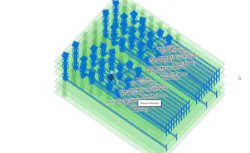
While standards-based analysis ensures basic interoperability, IBIS-AMI models allow for a more detailed prediction of real-world performance using advanced equalization and clock data recovery algorithms (Fig. 5). To navigate the vast number of design variables, AI-powered algorithms like the SHERPA algorithm are used to efficiently explore the design space, providing the fastest path to UCIe compliance with the fewest possible simulations.
Bringing It All Together with STCO
The fully floor-planned interposer and package substrate have now progressed through chiplet interface route planning, optimization, and predictive analysis, ensuring optimal power, performance, area, and cost tradeoffs. This is critical as it ensures the design meets all compliance requirements, thermal constraints, manufacturing, and testability readiness before physical implementation. Completing these steps reduces iteration cycles and accelerates time-to-production.
About the Author
Todd Burkholder
Senior Editor, Siemens Digital Industries Software
Todd Burkholder is a Senior Editor at Digital Industries Software. For over 30 years, he has worked as editor and author with internal and external customers to create print and digital content across a broad range of high-tech and EDA technologies. Todd began his career in marketing for high-technology and other industries in 1992 after earning a Bachelor of Science at Portland State University and a Master of Science degree from the University of Arizona.
Related
 Chiplets Stock Promo
 id_389914989__tatiana_golmer__dreamstime


Comment About the Article
To join the conversation, and become an exclusive member of Electronic Design, create an account today!
 Leaders Logo
Leaders relevant to this article: