How Dummy Silicon Helps Drive 3D Chip Innovation
What you'll learn:
- Why 3D ICs are harder to manufacture and test, and how stacking chiplets introduces new reliability challenges.
- How test vehicles and daisy-chain testing work, and how they’re evolving to validate 2.5D and 3D advanced packaging designs.
- How engineers use these tools to reduce risk, diagnose failures, and improve manufacturing processes before full-scale production.

In the fast-moving world of semiconductor manufacturing, innovation often outpaces established methods of verification and validation. The advent of 3D ICs adds to this challenge by stacking multiple layers of active devices, or chiplets, on top of each other in ultra-dense configurations. This approach introduces new manufacturing complexities and raises fresh questions about long-term reliability.
To help navigate this difficult terrain, the semiconductor industry has two specialized mechanisms: test vehicles and daisy-chain testing. This article explores how these approaches are used in practice and how they contribute to quality assurance in the arena of 3D ICs. More importantly, it shows why early, rigorous testing is not only helpful, but essential for reducing risk and bringing advanced packaging technologies to market.
Test Vehicles: What Are They and Why Do Engineers Use Them?
A test vehicle is a purpose-built semiconductor package, circuit board, or other structure that isn’t designed for commercial sale or direct product functionality. Instead, it’s used solely to evaluate and validate specific aspects of a manufacturing process or new technology.
Unlike a product intended for use in the real world, a test vehicle acts as a dedicated testbed, allowing engineers to probe the limits of the materials, processes, and designs being adopted under controlled conditions.
Such an approach is paramount when introducing new innovations into the semiconductor fabrication flow. These can include new bump and ball connections, the integration of components on unconventional organic substrates, or the embedding of chips directly within laminate materials.
Consider a scenario in which a manufacturer aims to integrate a chip within a complex laminate structure — perhaps for a cutting-edge wearable device. Before committing to the mass production of millions of units, which would entail significant investment and risk of costly delays, a test vehicle can be developed. This is used to validate the entire construction process of the device: creating the cavity, accurately placing the chip, and ensuring robust electrical connectivity within the laminate.
By verifying these critical processes early, companies can identify and resolve potential issues before full-scale production.
Daisy Chains: Testing High-Density Interconnects in 3D ICs
Within the broader landscape of chip prototyping, daisy-chain testing is a fundamental technique for assessing the integrity of electrical interconnections, particularly in advanced packaging configurations such as 3D ICs.
A daisy chain is an electrical circuit that connects multiple points, such as solder bumps connecting chiplets to a 2.5D package or micro-bumps between silicon dies stacked in 3D, in series. By creating a continuous path between them all, the configuration allows for a simple, yet highly effective, electrical resistance measurement spanning the entire chain.
While the test vehicle validates the entire manufacturing process, the daisy chain specifically verifies the electrical connectivity and mechanical integrity of interconnects within the subsystem (Fig. 1).
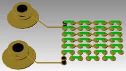
To illustrate, consider a flip-chip device — a common advanced packaging technique in which a semiconductor die is inverted and connected to a substrate through an array of solder bumps. As these assemblies undergo thermal cycling (repeated heating and cooling), differences in thermal expansion between the die and substrate can induce significant stress, particularly at the corner bumps. Over time, this stress may lead to micro-cracks or open connections.
While a manufacturer may be able to guarantee the reliability of connections for an 80,000-pin chip, all bets are off when a new design pushes the limit to 100,000 pins. How can the reliability of these additional, higher-density interconnections be confidently assessed?
A daisy-chain test vehicle addresses this dilemma by creating a continuous electrical path that traverses these critical interconnects. For instance, on the substrate, a trace might connect pin 1 to pin 2; on the die, a trace connects pin 2 to pin 3; then back to the substrate from pin 3 to pin 4, and so on, forming a literal chain through each bump and ball. The ends of this chain are then routed to a ball-grid-array (BGA) pad, which connects to test equipment.
>>Download the PDF of this article, and check out the TechXchange for similarly themed articles and videos

By measuring the total electrical resistance across this chain, any open circuit will result in an infinite resistance, immediately indicating a failure.
For more granular fault isolation, test vehicles often incorporate several shorter daisy chains, or include “taps” at intermediate points along a longer chain, routing these taps to separate BGA pads. If a main chain fails, resistance checks on these sub-chains or taps can pinpoint the approximate location of the open circuit.
That capability is invaluable for subsequent physical failure analysis. It enables engineers to precisely locate the defect through techniques like cross-sectioning or scanning acoustic microscopy, thus accelerating root cause identification and process improvement.
The Many Faces of Test Vehicles
The responsibility for building these test systems is often shared by different players within the semiconductor ecosystem. Manufacturers, including outsourced semiconductor assembly and test (OSAT) firms and foundries, frequently develop test vehicles in-house to validate their proprietary processes and guarantee performance specifications.
For instance, if a foundry claims the ability to reliably produce 12-micron line and space features with an 80,000-pin die, they will probably use internal test vehicles to substantiate these claims and qualify their processes.
However, as customers push the boundaries of what’s currently manufacturable, the onus can shift. When designers create a product with a 120,000-pin die, exceeding the manufacturer's standard guarantees, they may need to commission or design their own test vehicles.
In such cases, the “die” is typically a “dummy die” — an inert silicon piece featuring only a redistribution layer with the necessary electrical connections for the daisy chain or other test structures, rather than active circuitry. This dummy die mimics the physical characteristics of the actual product without the complexity or cost of fabricating functional transistors.
Layout engineers, who are responsible for the physical design of chips and packages, are the primary architects of these test vehicles. They translate the specific validation requirements into physical designs, ensuring that the test structures accurately represent the critical features and potential failure modes of the target product.
It’s common for large customers to develop several test vehicles, sometimes 10 to 12 for every product, to comprehensively evaluate various aspects of manufacturing — from interconnect reliability to thermal performance — across different process variations.
This collaborative and often iterative process between manufacturers and customers is essential for lowering the risk of advanced packaging innovations.
Heat, Comb, Stack: Testing the Physical Limits of 2.5D and 3D Chips
With the “Wild West” nature of the 3D IC space, companies are rapidly developing new ways of doing heterogeneous integration. As a result, test vehicles must incorporate increasingly advanced structures that go above and beyond the daisy chain.
This is increasingly critical when it comes to validating silicon bridges used for die-to-die interfaces. In many 3D IC designs, a silicon bridge — a small silicon interposer — is employed to connect multiple chiplets (such as an ASIC or HBM) arranged on an organic substrate. This bridge is typically flipped, with its pins oriented upwards, allowing the chiplets to align and connect precisely to it.
The manufacturing process for aligning and bonding these components is highly complex. To evaluate it, a test vehicle can include a dummy silicon bridge and dummy chiplets, all designed with daisy-chain structures that traverse the critical interconnects.
In turn, engineers can quickly verify the physical and electrical integrity of the bridge connections without the need for functional, live chips that would require more complex full-speed testing. If a manufacturing process is changed, a quick run with this test vehicle can confirm its efficacy without risking expensive functional prototypes.
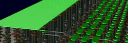
Furthermore, test vehicles can be equipped with structures that simulate real-world stresses during operation and detect subtle manufacturing defects (Fig. 2).
For instance, while a daisy chain is able to measure resistance, advanced test vehicles often also include:
- Heaters: These are resistive patterns embedded within the substrate that generate localized heat.
- By incorporating heaters, engineers can simulate the thermal stresses experienced by interconnections under operational load. This allows for accelerated lifetime testing and the identification of interconnect failures caused by coefficient of thermal expansion mismatches under conditions that mimic actual device operation.
- Comb structures: These interdigitated patterns are designed to detect capacitive discharge.
- They’re highly sensitive to residual contaminants, such as flux residue or other process byproducts, that might be left on the device after mounting or cleaning processes. These residues can lead to leakage currents or even short circuits, compromising device reliability. By measuring the capacitance or leakage current across these comb structures, manufacturers are able to assess the cleanliness and integrity of their assembly processes.
- Stacked via chains: The ability to stack vias directly on top of each other across multiple layers is crucial for achieving high routing density in 3D ICs.
- However, stacked vias are highly susceptible to manufacturing misregistration when successive layers aren’t perfectly aligned. Test vehicles address this by incorporating multiple daisy chains, each with a controlled degree of via misregistration. For example, one chain might have perfectly aligned stacked vias, while subsequent chains have vias intentionally offset by 5, 10, or even 15 microns.
- By testing these chains, engineers can determine the maximum allowable misregistration before connectivity is lost, establishing critical design rules and process windows.
These advanced components give engineers a way to probe the limits of modern manufacturing processes. They can be used to qualify new materials, fine-tune parameters, and ultimately ensure robust, reliable performance for 3D IC designs.
By measuring resistance, daisy chains provide a simple pass/fail check on connectivity. But the true value of test vehicles lies in the ability to provide a diagnostic look into the design. Engineers can use these insights to pinpoint failure mechanisms and guide process improvements.
For example, the use of heaters allows engineers to understand how interconnects behave under thermal stress, which is a primary driver of failure in advanced packaging (Fig. 3). If corner bumps are consistently failing under simulated operational temperatures, the data from the heated test vehicle can guide adjustments to underfill materials, bonding processes, or package design to mitigate these stresses.
Similarly, comb structures provide direct feedback on the efficacy of cleaning protocols. This helps identify and eliminate sources of contamination that could lead to latent defects or early field failures.
The ability to stack vias directly rather than having to offset — or “dog-bone” — them around obstacles is a boon to routing density and overall package size reduction. However, each layer in a multi-layer substrate has its own registration tolerances, and accumulating these tolerances can lead to misaligned vias. By designing test vehicles with chains of vias intentionally misaligned by varying degrees, manufacturers can empirically determine the maximum permissible misregistration before electrical continuity is compromised.
This data can be invaluable for setting robust design rules and ensuring that production yields remain high even with tight pitch requirements. These insights are critical for pushing the boundaries of what’s manufacturable while maintaining high reliability.
Don’t Go It Alone: EDA Tools Evolve to Help with Heterogeneous Integration
Despite the sophisticated capabilities of current test vehicles, the rapid evolution of 3D ICs continues to present new challenges and opportunities for innovation in testing. One significant area for improvement lies in the automation of test-vehicle design, particularly for daisy-chain structures.
Currently, it’s not uncommon for design engineers to manually create daisy-chain netlists. Because a single electrical net in a design tool typically connects all pins with the same name, creating a serial daisy chain requires breaking the continuous path into discrete, uniquely named segments (e.g., Fred_1, Fred_2, and Fred_3). This manual process, often involving spreadsheets and painstaking netlist manipulation, is prone to human error as well as being time-consuming and inefficient.
As 3D IC designs become increasingly complex with hundreds of thousands or even millions of interconnects, manual daisy-chain generation becomes an unsustainable bottleneck.
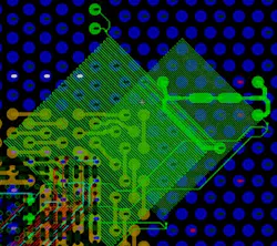
Fortunately, the industry is moving toward more intelligent EDA tools that can automate the creation of these complex test structures. These tools leverage advanced algorithms to generate daisy-chain patterns, comb structures, and stacked via arrays directly from design specifications, ensuring accuracy and significantly reducing design cycle time (Fig. 4).

Moreover, these tools can integrate with simulation environments to predict the electrical and thermal performance of the test structures, providing a more comprehensive validation strategy.
As 3D IC technology matures, the demand for even more integrated and predictive test-vehicle solutions will grow. This includes the development of multi-physics simulation capabilities that can accurately model the interplay of thermal, mechanical, and electrical stresses within complex 3D structures, guiding the design of more effective test vehicles.
The future of 3D IC validation will undoubtedly involve a tighter integration of design, simulation, and physical testing. It will help ensure that the promise of advanced packaging can be realized with unwavering reliability and manufacturability.
For those still relying on manual methods, the message is clear: Leverage the evolving capabilities of EDA tools to streamline test vehicle design and accelerate the path to robust 3D IC products.
Test Driving Reliability and Performance
Ultimately, test vehicles serve as an economical and efficient means to validate critical manufacturing steps without the prohibitive cost and complexity of using functional product dies. They allow for the isolation of specific process variables and precise characterization of their impact on reliability.
This targeted approach is essential for ensuring that 3D IC designs meet the rigorous quality and performance standards demanded by the industry. It will also prevent costly recalls and maintain customer trust.
>>Download the PDF of this article, and check out the TechXchange for similarly themed articles and videos
About the Author
Todd Burkholder
Senior Editor, Siemens Digital Industries Software
Todd Burkholder is a Senior Editor at Digital Industries Software. For over 30 years, he has worked as editor and author with internal and external customers to create print and digital content across a broad range of high-tech and EDA technologies. Todd began his career in marketing for high-technology and other industries in 1992 after earning a Bachelor of Science at Portland State University and a Master of Science degree from the University of Arizona.
Kendall Hiles
Senior 3D IC Product Specialist, Siemens EDA
Kendall Hiles is a distinguished Senior 3D IC Product Specialist at Siemens EDA, bringing four decades of experience in electronic design automation. His unique perspective stems from his experience working across multiple technological transitions in the semiconductor industry, from traditional IC design to modern 3D IC implementation.
Comment About the Article
To join the conversation, and become an exclusive member of Electronic Design, create an account today!

Leaders relevant to this article: